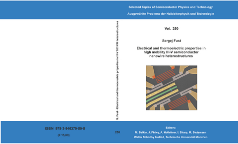
Electrical and thermoelectric properties in high mobility III-V semiconductor nanowire heterostructures
Seiten
2023
Verein zur Förderung des Walter Schottky Instituts der Technischen Universität München (Verlag)
978-3-946379-50-8 (ISBN)
Verein zur Förderung des Walter Schottky Instituts der Technischen Universität München (Verlag)
978-3-946379-50-8 (ISBN)
- Titel nicht im Sortiment
- Artikel merken
In view of the ever-increasing challenges related to energy consumption and the impact on the environment it is causing, new approaches must be taken. The application of the thermoelectric effect for this purpose would be a promising approach, as it can convert excess heat into electricity and thus, into easily usable energy. The problem lies in the interdependency of several parameters determining thermoelectric power conversion efficiency, such that it is not possible to change one parameter without affecting the others. However, one way out of this dilemma could be the exploitation of thermoelectric materials in lower dimensions at the nanoscale. There, the relevant parameters such as electrical and thermal conductivity, and Seebeck coefficient as well as thermopower are no longer so strongly connected with each other, and an independent control of the parameters would be possible. The goal of this work is to build a platform that allows testing specific low-dimensional semiconductor materials, namely 1D-nanowires for their applicability in the field of thermoelectrics. For this purpose, two different material systems were investigated, GaAs and InAs based nanowires. The first part of the thesis deals with the growth and analysis of advanced modulation doped GaAs-AlGaAs core-shell nanowires. The GaAs-core is thinned down to a diameter of 10-30nm by in-situ annealing to get into the 1D quantum confinement regime. Additionally, a Si delta-doping layer is introduced during the shell growth, to increase the charge carrier density without hampering the mobility and to form a high-mobility free electron gas. Afterwards, the electrical, thermoelectric and thermal transport properties are investigated. For this purpose, field effect transistors (FET) are fabricated using a Schottky barrier top-gate. Normally-on n-type transistor characteristics are observed for the temperature range from room temperature down to 4.2K. Nearly no hysteresis is observed, signaling an excellent interface quality between the wire and the gate contact. Increasing mobility with decreasing temperature is shown, evidencing the reduced phonon scattering, reaching values of up to 1300 cm2/Vs and a sheet charge carrier density in the range of 3×1012 cm-2. At the lowest temperature conductance quantization is apparent, by showing a step-like increase of the conductance, with a 1D-diffusive transmission probability of 0.2 measured on a single device. Subsequently, the Seebeck coefficient is determined by creating and measuring a temperature gradient along the wire, and recording the resulting Seebeck voltage. A Seebeck voltage of up to 0.4mV is observed, appearing at positions nicely coinciding with the plateau onset in the conductance trace. This is expected, as the Seebeck coefficient is strongly correlated to the change of the density of states (DOS), which is especially pronounced in a 1D-conductor at the sub-band edges. A Seebeck coefficient of up to −83 μVK-1 can be extracted, resulting in a thermopower of up to 60 μWm-1K-1. As the thermopower is the combination of the Seebeck coefficient and the conductivity of the charge carriers, the maximum value for it is found not in the sub-band with the highest Seebeck coefficient, but in a higher sub-band, due to the strong increase of conductivity with increasing sub-band number. The thermal conductivity measured on several nanowires using µ-Raman spectroscopy shows very low values as low as 3 Wm-1K-1 which depends on core-diameter under the given core-shell geometrical design. This is nearly one order of magnitude lower as the literature values for bulk GaAs and unpassivated GaAs nanowires. The second part of the thesis is dedicated to the transport investigation of InAs-based nanowires. First, transport properties of pure, unpassivated InAs wires present the current state of the art. Back-gated FET structures allow to extract the mobility, ranging from 600 cm2/Vs at room temperature up to 1700 cm2/Vs at cryogenic temperatures for wires with a diameter of around 100 nm. Typical charge carrier densities of such nanowires are on the order of 1.5E+17 cm-3, as measured at room temperature. At temperatures below 70 K, current modulation in the transfer curves demonstrates the appearance of conductance quantization at temperatures way above the ones observed in GaAs wires. Even for channel lengths of up to 1 μm nicely resolved steps are observable, accounting for an increased transmission probability of ca. 0.33. Further on, InAs wires are overgrown with a newly developed and nearly lattice-matched AlSb shell to passivate the core. In specific InAs-AlSb core-shell NWs, also an InAs QW is grown inside the shell, which is necessary to introduce n-type doping with Si in an AlSb environment. Here, a new contact metallization is developed, consisting of a Ti/Pd/Pt/Au stacking layer followed by a temperature treatment at 150 °C. As the electrical measurements show characteristics pointing towards the formation of a parasitic channel in the QW, core-shell wires without intentionally doped QWs are investigated. While the used metal layers are the same, an additional temperature increase to 300 °C of the annealing step is necessary, to create ohmic contacts since the core is buried further away from the NW surface, resulting in 2-terminal resistances down to 10 kOhm. From transfer curves of 2-terminal devices, estimates of mobilities and conductivities of the same magnitude as in pure InAs wires are observed in the InAs-AlSb wires. The absence of a strong mobility increase in passivated wires hints towards strain induced defects, limiting the overall performance. Additionally, even above temperatures of 100 K, conductance steps are still visible. A transmission probability of up to 0.4 is observed at 80K for a 700nm long channel. Preliminary thermal conductivity measurements on as-grown InAs nanowires are also performed as a first stepping stone towards full thermoelectric characterization, with the data presented in the Appendix. The observation of distinct 1D-like conductance behavior even at elevated temperatures clearly shows the potential of nanowires for the thermoelectric power generation. With the utilization of the correct materials and a sophisticated design, manipulation of the density of states in such 1D-conductors that lead to a significant increase in the Seebeck coefficient, may enable the increase of the figure of merit beyond the limits present in bulk systems.
| Erscheinungsdatum | 29.08.2023 |
|---|---|
| Sprache | englisch |
| Maße | 150 x 210 mm |
| Themenwelt | Naturwissenschaften ► Physik / Astronomie |
| Schlagworte | nanowire • semiconductor • Thermoelectric |
| ISBN-10 | 3-946379-50-8 / 3946379508 |
| ISBN-13 | 978-3-946379-50-8 / 9783946379508 |
| Zustand | Neuware |
| Haben Sie eine Frage zum Produkt? |
Mehr entdecken
aus dem Bereich
aus dem Bereich
von den Werkzeugen über Methoden zum TQM
Buch | Softcover (2024)
Springer Fachmedien (Verlag)
32,99 €
kurz und praktisch - für Ingenieure und Naturwissenschafler
Buch | Softcover (2024)
De Gruyter Oldenbourg (Verlag)
44,95 €


