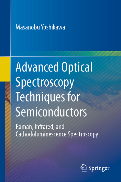
Advanced Optical Spectroscopy Techniques for Semiconductors
Springer International Publishing (Verlag)
978-3-031-19721-5 (ISBN)
Dr. Masanobu Yoshikawa completed his doctorate in applied spectroscopy with the Fourier transform infrared (FT-IR) and Raman spectroscopy at the Osaka University in 1986. After his analytical study of the one-dimensionally conducting metal-tetracyanoquinodimethanide (M-TCNQ) with FT-IR and Raman spectroscopy at the Osaka University, he joined Toray Research Center, Inc. in 1986, which is a leading analytical service company in Japan. He has mainly studied wide-gap semiconductors such as diamond, gallium nitride, silicon carbide, using FT-IR, Raman, and cathodoluminescence. He worked for Fraunhofer-Institute in Freiburg in Germany for 6 months in 1998. Furthermore, he has served as the Japanese national project leader for development of the world-first scanning near field Raman spectroscopy (SNOM) from 2003 to 2007, entrusted by New Energy and Industrial Technology Development Organization (NEDO) in Japan and succeeded in stress characterization of Si devices with a spatial resolution of less than 100 nm. As a result, he was awarded the Advance Analytical Instrument Development prize from the Japan Society for Analytical Chemistry (JAIMA) in 2010. He is working for Toray Research Center, Inc. as a senior vice-president and a senior fellow.
1. Introduction.- 2. Raman and infrared (IR) spectroscopy.- 3. Photoluminescence (PL) spectroscopy.- 4. Overview of cathodoluminescence (CL) spectroscopy.- 5. Applications of Raman, IR, and CL spectroscopy.- 6. STEM-CL spectroscopy.- 7. Topics.- Index.
| Erscheinungsdatum | 25.03.2023 |
|---|---|
| Zusatzinfo | XI, 223 p. 178 illus., 131 illus. in color. |
| Verlagsort | Cham |
| Sprache | englisch |
| Maße | 155 x 235 mm |
| Gewicht | 510 g |
| Themenwelt | Naturwissenschaften ► Physik / Astronomie ► Atom- / Kern- / Molekularphysik |
| Technik ► Elektrotechnik / Energietechnik | |
| Technik ► Maschinenbau | |
| Schlagworte | Characterization of Semiconductors • Crystal Orientation Characterization • Gallium Arsenide Devices • Indium Phosphate Devices • Michelson Interferometer • Nano-Diamond Thin Films • Scanning Electron Transmission Microscopy • Scanning Near-field Optical Microscopy • Spectroscopy of Semiconductors • Strained Silicon • Stress Determination Using Raman Spectroscopy • Terahertz time-domain spectroscopy • vibrational spectroscopy |
| ISBN-10 | 3-031-19721-6 / 3031197216 |
| ISBN-13 | 978-3-031-19721-5 / 9783031197215 |
| Zustand | Neuware |
| Haben Sie eine Frage zum Produkt? |
aus dem Bereich


