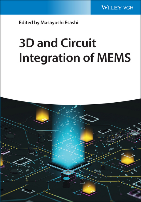
3D and Circuit Integration of MEMS
Wiley-VCH (Verlag)
978-3-527-34647-9 (ISBN)
Masayoshi Esashi is Professor in the Micro System Integration Center at Tohoku University, Japan. He obtained his PhD from Tohoku University and has been working there as a researcher and teacher. His research interests include MEMS, integrated sensors and MEMS packaging. He has published more than 500 scientific papers and has received numerous awards including the IEEE Andrew S. Grove Award in 2015 and IEEE Jun-ichi Nishizawa medal in 2016.
PART I INTRODUCTION
1 OVERVIEW
PART II SYSTEM ON CHIP
2. BULK MICROMACHINING
2.1 Process Basis of Bulk Micromachining Technologies
2.2 Bulk micromachining based on wafer bonding
2.3 Single wafer single side processes
3. ENHANCED BULK MICROMACHINING BASED ON MIS PROCESS
3.1 Repeating MIS cycle for multi-layer 3D structure or multi-sensor integration
3.2 Pressure sensor fabrication - - from MIS updated to TUB
3.3 Extension of MIS process for various advanced MEMS devices
4. EPITAXIAL POLY SI SURFACE MICROMACHINING
4.1 Process condition of epi-poly Si
4.2 MEMS devices using epi-poly Si
5. POLY SIGE SURFACE MICROMACHINING
5.1 Introduction
5.2 SiGe deposition
5.3 LP CVD polycrystalline SiGe
5.4 CMEMS¿ process
5.5 Poly-SiGe applications
6. METAL SURFACE MICROMACHINING
6.1 Background of Surface Micromachining
6.2 Static device
6.3 Static structure fixed after the single movement
6.4 Dynamic device
6.5 Summary
7. HETEROGENEOUSLY INTEGRATED ALUMINUM NITRIDE MEMS RESONATORS AND FILTERS
7.1 Overview of integrated aluminum nitride MEMS
7.2. Heterogeneous integration of aluminum nitride MEMS resonators with CMOS circuits
7.3 Heterogeneously integrated self-healing filters
8. MEMS USING CMOS WAFER
8.1 Introduction : CMOS MEMS architectures and advantages
8.2 Process modules for CMOS MEMS
8.3 The 2P4M CMOS platform (0.35µm)
8.4 The 1P6M CMOS platform (0.18µm)
8.5 CMOS MEMS with add-on materials
8.6 Monolithic integration of circuits and sensors
8.7 Issues and Concerns
8.8 Concluding remarks
9. WAFER TRANSFER
9.1 Introduction
9.2 Film transfer
9.3 Device transfer (Via-last)
9.4 Device transfer (via-first)
9.5 Chip level transfer
10. PIEZOELECTRIC MEMS
10.1 Introduction
10.2 PZT thin film deposition
10.3 PZT-MEMS fabrication process
PART III BONDING, SEALING AND INTERCONNECTION
11. ANODIC BONDING
11.1 Principle
11.2 Distortion
11.3 Influence of anodic bonding to circuits
11.4 Anodic bonding with various materials, structures and conditions
12. DIRECT BONDING
12.1 Wafer direct bonding
12.2 Hydrophilic wafer bonding
12.3 Surface activated bonding at room temperature
13. METAL BONDING
13.1 Solid liquid inter-diffusion bonding (SLID)
13.2 Metal Thermocompression bonding
13.3 Eutectic bonding
14. REACTIVE BONDING
14.1 Motivation
14.2 Fundamentals of reactive bonding
14.3 Material systems
14.4 State of the art
14.5 Deposition concepts of reactive material systems
14.6 Bonding with RMS
14.7 Conclusion
15. POLYMER BONDING
15.1 Introduction
15.2 Materials for polymer wafer bonding
15.3 Polymer wafer bonding technology
15.4 Precise wafer-to-wafer alignment in polymer wafer bonding
15.5 Practical examples of polymer wafer bonding processes
15.6 Summary and Conclusions
16. SOLDERING BY LOCAL HEATING
16.1 Soldering in MEMS packaging
16.2 Laser soldering
16.3 Resistive heating and soldering
16.4 Inductive heating and soldering
16.5 Other localized soldering processes
17. PACKAGING, SEALING AND INTERCONNECTION
17.1 Wafer level packaging
17.2 Sealing
17.3 Interconnection
18. VACUUM PACKAGING
18.1 Problems of vacuum packaging
18.2 Vacuum packaging by anodic bonding
18.3 Packaging by anodic bonding with controlled cavity pressure
18.4 Vacuum packaging by metal bonding
18.5 Vacuum packaging by deposition
18.6 Hermeticity testing
19. BURIED CHANNELS IN MONOLITHIC SI
19.1 Buried channel/cavity in LSI and MEMS
19.2 Monolithic SON technology and related technologies
19.3 Applications of SON
20. THROUGH-SUBSTRATE-VIAS
20.1 Configuration of TSVs
20.2 TSV applications in MEMS
20.3 Considerations for TSV in MEMS
20.4 Fundamental TSV fabrication technologies
20.5 Polysilicon TSVs
20.6 Silicon TSVs
20.7 Metal TSVs
| Erscheinungsdatum | 21.04.2021 |
|---|---|
| Verlagsort | Weinheim |
| Sprache | englisch |
| Maße | 170 x 244 mm |
| Gewicht | 1130 g |
| Themenwelt | Naturwissenschaften ► Chemie |
| Technik ► Elektrotechnik / Energietechnik | |
| Technik ► Maschinenbau | |
| Schlagworte | Electrical & Electronics Engineering • Electronic materials • Elektronische Materialien • Elektrotechnik u. Elektronik • Halbleiterphysik • Materials Science • Materialwissenschaften • MEMS • Physics • Physik • Semiconductor physics |
| ISBN-10 | 3-527-34647-3 / 3527346473 |
| ISBN-13 | 978-3-527-34647-9 / 9783527346479 |
| Zustand | Neuware |
| Informationen gemäß Produktsicherheitsverordnung (GPSR) | |
| Haben Sie eine Frage zum Produkt? |
aus dem Bereich


