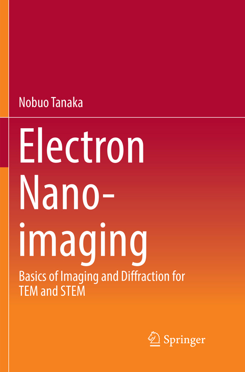
Electron Nano-Imaging
Springer Verlag, Japan
978-4-431-56804-9 (ISBN)
Dr. Nobuo Tanaka is a designated professor of Institute of Materials and Systems for Sustainability (IMaSS) of Nagoya University and an adjunct senior researcher of Japan Fine Ceramic Center (JFCC). He received a ph.D degree from Applied Physics Department of Nagoya University in 1978, and became an assistant professor of the department. He stayed Arizona State University as a visiting scholar to study with the late Prof. J. Cowley from 1983 to 1985. He was appointed a full professor of Applied Physics of Nagoya University in 1999 through an associate professor. In 2001, he moved to Center of Integrated Research for Science and Engineering (CIRSE) of Nagoya University, which was renamed EcoTopia Science Institute (ESI) in 2004. He was the director of the institute from 2012 to 2015. He is also the president of Japanese Microscopy Society (JSM) from 2015 to 2017. His professionals are high-resolution electron microscopy and nano-diffraction, and physics of atomic clusters and thin filmsas well as surfaces and interfaces of semiconductors. He is also the editor/author of a textbook as Scanning Transmission Electron Microscopy of Nanomaterials.
Seeing nanometer-sized world.- Structure and imaging of a transmission electron microscope (TEM).- Basic theories of TEM imaging.- Resolution and image contrast of a transmission electron microscope (TEM).- What is high-resolution transmission electron microscopy ?.- Lattice images and structure images.- Imaging theory of high-resolution TEM and image simulation.- Advanced transmission electron microscopy.- What is scanning transmission electron microscopy (STEM)?.- Imaging of scanning transmission electron microscopy (STEM).- Image contrast and its formation mechanism in STEM.- Imaging theory for STEM.- Future prospects and possibility of TEM and STEM.- Concluding remarks.- Introduction of Fourier transforms for TEM and STEM.- Imaging by using a convex lens: Convex lens as phase shifter.- Contrast transfer function of a transmission electron microscope: Key term for understanding of phase contrast in HRTEM.- Complex-valued expression of aberrations of a round lens.- Cowley's theoryfor TEM and STEM imaging.- Introduction to the imaging theory for TEM including non-linear terms.- What are image processing methods?.- Elemental analysis by electron microscopes: Analysis using an electron probe.- Electron beam damage to specimens.- Scattering of electrons by an atom: Fundamental process for visualization of a single atom by TEM.- Electron diffraction and convergent beam electron diffraction (CBED): Basis for formation of lattice fringes in TEM and image intensity of STEM.- Bethe's method for dynamical electron diffraction: Basic theory of electron diffraction in thicker crystals.- Column approximation and Howie-Whelan's method for dynamical electron diffraction: Theory for observation of lattice defects.- Van-Dyck's method for dynamical electron diffraction and imaging: Basis of atomic column imaging.- Eikonal theory for scattering of electrons by a potential.- Debye-Waller factor and thermal diffuse scattering (TDS).- Relativistic effects to diffraction and imagingby a transmission electron microscope: Basic theories for high-voltage electron microscopy.
“I enjoyed reading this book. It covers a wide range of applications, from basics on electron microscopy and diffraction, to more advanced, newly developed techniques for imaging and diffraction. … I strongly recommend this book as a resource for electron microscopists with a basic knowledge of TEM and STEM who are interested in advanced imaging and diffraction techniques.” (Lourdes Salamanca-Riba, MRS Bulletin, Vol. 43, May, 2018)
| Erscheinungsdatum | 27.08.2018 |
|---|---|
| Zusatzinfo | 22 Illustrations, color; 107 Illustrations, black and white; XXVIII, 333 p. 129 illus., 22 illus. in color. |
| Verlagsort | Tokyo |
| Sprache | englisch |
| Maße | 155 x 235 mm |
| Themenwelt | Naturwissenschaften ► Chemie ► Analytische Chemie |
| Naturwissenschaften ► Physik / Astronomie ► Festkörperphysik | |
| Technik ► Maschinenbau | |
| Schlagworte | Bethe Method • Cowley's Theory • Electron Wave Optics • Energy-filtered Transmission Electron Microscopy • High-resolution Electron Microscopy • Howies–Whelan Method • Lattice Fringe Images • Magnetic Lenses • Van Dyck Method |
| ISBN-10 | 4-431-56804-2 / 4431568042 |
| ISBN-13 | 978-4-431-56804-9 / 9784431568049 |
| Zustand | Neuware |
| Informationen gemäß Produktsicherheitsverordnung (GPSR) | |
| Haben Sie eine Frage zum Produkt? |
aus dem Bereich


