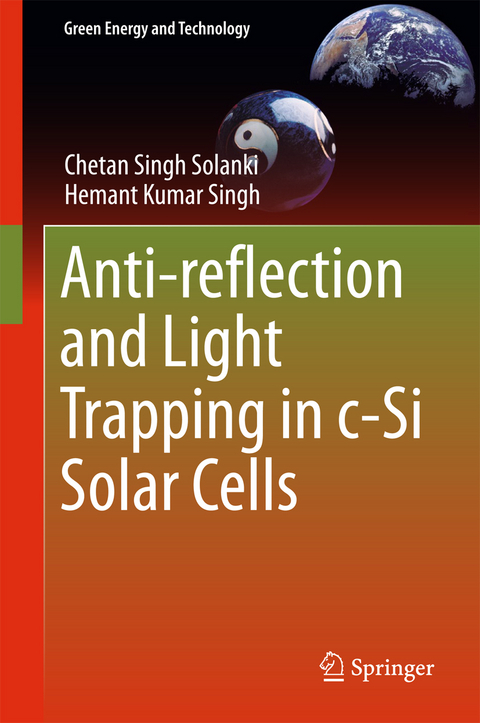
Anti-reflection and Light Trapping in c-Si Solar Cells (eBook)
XXIX, 186 Seiten
Springer Singapore (Verlag)
978-981-10-4771-8 (ISBN)
Dr. Chetan Singh Solanki is currently a professor at the Department of Energy Science and Engineering at the Indian Institute of Technology Bombay (IITB), India. He is an expert on crystalline Si technology, Si-nanostructures (including quantum dots), thin film Si solar cells, PV concentrator systems and carbon nanotubes. He received his Ph.D. from the specialist silicon laboratory, IMEC (Inter-university Micro-electronics Center, Catholic University of Leuven, Belgium). He has worked on several state-sponsored and private-sector projects exploring crystalline Si solar cells, both wafer based and thin film nanomaterial based variants. The Ministry of New and Renewable Energy has sponsored a project titled 'National Center for Photovoltaic Research and Education (NCPRE)', in which he is one of the Principal Investigators. He is also one of the Principal Investigators of 'Localization of Solar Energy through Local Assembly, Sale and Usage of 1 Million Solar Urja Lamps (SoUL)'. He has been the recipient of many awards as an investigator, has authored several books on solar PV and more than 100 international and national publications, and holds 11 patents.
Dr. Hemant Kumar Singh has more than six years of experience in the research and development of Solar Photovoltaic Technologies. He also has industry experience of in-line 6 inch multi c-Si wafer based solar cell manufacturing. Dr. Singh worked towards his Ph.D. thesis at the Department of Energy Science and Engineering (DESE) under the MNRE, Government of India funded project 'National Center for Photovoltaic Research and Education (NCPRE)' at the IIT Bombay, India. His R & D work was in fabrication and characterization of solar cells. His Ph.D. thesis focused on plasmonics based advanced light trapping structures for next-generation thin c-Si solar cell applications. Prior to his Ph.D., he completed his M.Tech in Solid State Technology from IIT Kharagpur, West Bengal, India. During his M.Tech course, his research focus was on CIGS-CdS based hetero-junction for solar applications. He also holds an M.Sc. degree in Physics with a specialization in Electronics from D.D.U. Gorakhpur University, Gorakhpur, Uttar Pradesh, India.
This book offers essential insights into c-Si based solar cells and fundamentals of reflection, refraction, and light trapping. The basic physics and technology for light trapping in c-Si based solar cells are covered, from traditional to advanced light trapping structures. Further, the book discusses the latest developments in plasmonics for c-Si solar cell applications, along with their future scope and the requirements for further research. The book offers a valuable guide for graduate students, researchers and professionals interested in the latest trends in solar cell technologies.
Dr. Chetan Singh Solanki is currently a professor at the Department of Energy Science and Engineering at the Indian Institute of Technology Bombay (IITB), India. He is an expert on crystalline Si technology, Si-nanostructures (including quantum dots), thin film Si solar cells, PV concentrator systems and carbon nanotubes. He received his Ph.D. from the specialist silicon laboratory, IMEC (Inter-university Micro-electronics Center, Catholic University of Leuven, Belgium). He has worked on several state-sponsored and private-sector projects exploring crystalline Si solar cells, both wafer based and thin film nanomaterial based variants. The Ministry of New and Renewable Energy has sponsored a project titled “National Center for Photovoltaic Research and Education (NCPRE)”, in which he is one of the Principal Investigators. He is also one of the Principal Investigators of “Localization of Solar Energy through Local Assembly, Sale and Usage of 1 Million Solar Urja Lamps (SoUL)”. He has been the recipient of many awards as an investigator, has authored several books on solar PV and more than 100 international and national publications, and holds 11 patents. Dr. Hemant Kumar Singh has more than six years of experience in the research and development of Solar Photovoltaic Technologies. He also has industry experience of in-line 6 inch multi c-Si wafer based solar cell manufacturing. Dr. Singh worked towards his Ph.D. thesis at the Department of Energy Science and Engineering (DESE) under the MNRE, Government of India funded project “National Center for Photovoltaic Research and Education (NCPRE)” at the IIT Bombay, India. His R & D work was in fabrication and characterization of solar cells. His Ph.D. thesis focused on plasmonics based advanced light trapping structures for next-generation thin c-Si solar cell applications. Prior to his Ph.D., he completed his M.Tech in Solid State Technology from IIT Kharagpur, West Bengal, India. During his M.Tech course, his research focus was on CIGS-CdS based hetero-junction for solar applications. He also holds an M.Sc. degree in Physics with a specialization in Electronics from D.D.U. Gorakhpur University, Gorakhpur, Uttar Pradesh, India.
Preface 6
Acknowledgements 9
Contents 10
About the Authors 14
List of Figures 15
1 Solar Cells Overview and Perspective to Light-Trapping Schemes 28
1.1 Place of Solar PV Technology in World Energy Mix 28
1.2 Historical Development of Solar Cells 30
1.3 Different Solar Cell Technologies 32
1.4 Current Status of Solar Cell Technologies 33
1.5 Basic Working Principle of Solar Cells 35
1.6 Why c-Si Solar Cell? 37
1.7 Importance of Light-Trapping Structure 39
1.8 Questions and Problems 42
References 42
2 c-Si Solar Cells: Physics and Technology 44
2.1 Overview of c-Si Solar Cells 44
2.2 c-Si Solar Cell: Design and Technology 46
2.2.1 Classification of c-Si-Based Solar Cells 46
2.2.2 Architecture of c-Si Solar Cells 48
2.2.3 Historical Development 50
2.3 Manufacturing Process of c-Si Solar Cells 53
2.4 Photovoltaic Effect in c-Si Solar Cells and Important Parameters 56
2.4.1 Photovoltaic Effect in c-Si Solar Cells 56
2.4.2 Current–Voltage Characteristics 57
2.4.3 Important Solar Cell Parameters 59
2.4.3.1 Open Circuit Voltage (Voc) 59
2.4.3.2 Short Circuit Current (Jsc) 59
2.4.3.3 Maximum Power (Pmax) 59
2.4.3.4 Fill Factor (FF) 60
2.4.3.5 Efficiency (?) 60
2.4.3.6 Quantum Efficiency (QE) 60
2.5 Role of Light-Trapping Structures 62
2.6 ITRPV Roadmap for c-Si Solar Cell Development 64
2.7 Next Generation c-Si Solar Cells 65
2.8 Questions and Problems 67
References 68
3 Principle of Dielectric-Based Anti-reflection and Light Trapping 70
3.1 Reflection, Refraction, and Transmission from Dielectric Interfaces 70
3.1.1 Reflection, Refraction, and Transmission 70
3.1.2 Wave Optics Based Interaction of Light with Dielectric Medium and Interfaces 72
3.1.3 Fresnel Equations for Reflection and Transmission 73
3.2 Dielectric Thin Films and Their Role in Reflection Reduction 76
3.3 Role of Refractive Index and Dielectric Medium 79
3.4 Multilayer Dielectric Thin Films for Reflection Reduction 82
3.5 Additional Functionality of Dielectric Anti-reflection Layers 86
3.6 Limitation of Dielectric-Based Anti-reflection Structure 88
3.7 Questions and Problems 90
References 91
4 Principle of Texturization for Enhanced Light Trapping 92
4.1 Surface Morphology and Its Impact on Light Reflection, Refraction and Transmission 92
4.2 Textured Surfaces in c-Si Solar Cells 96
4.3 Role of Texture Size and Shape in Light Trapping and Reflection Reduction 99
4.4 Single Side Texturing Versus Both Side Texturing 102
4.5 Most Suitable Textured Surface for Better Light Trapping 103
4.6 Implication of Texturing Based Light Trapping Structure 107
4.7 Questions and Problems 108
References 109
5 Texturing Process of c-Si Wafers 110
5.1 Si Crystal Structure 110
5.2 Wafer Type and Orientation for c-Si Solar Cell Fabrication 113
5.3 Chemical Process for Texturing 116
5.4 Process Control for Texture Pyramids Size and Shape Distribution 120
5.5 Industrial Processes Used for Surface Texturing 121
5.6 Practical Implications of Chemical Texturing Processes 122
5.7 Questions and Problems 123
References 123
6 Anti-reflection Coatings with Textured Surface for c-Si Solar Cells 125
6.1 Primary Benefit of Textured Surface in Combination with Anti-reflection Layer 125
6.2 Analysis on Cell Performance Having Textured Surface but Without and with Anti-reflection Layer 129
6.3 Dual Role of Anti-reflection Layers in c-Si Solar Cells 131
6.4 Most Suitable Light Trapping Geometry 133
6.5 Implication of Existing Light Trapping Geometry for Next Generation Solar Cells 135
6.6 Suitable Light Trapping Structure for Next Generation Solar Cells 136
6.7 Questions and Problems 138
References 140
7 Advancements in Traditional Light Trapping Structures 141
7.1 Traditional Light-Trapping Structures 141
7.2 Inverted Pyramid-Based Light Trapping for Thin Wafer-Based Cells 144
7.3 Back Reflectors for Enhanced Light Trapping 146
7.4 Advanced Light-Trapping Structures for Next-Generation c-Si Solar Cells 149
7.5 Questions and Problems 150
References 151
8 Plasmonic-Based Advanced Anti-reflection and Light Trapping: Principles and Technology 152
8.1 Plasmonics: Historical Development 152
8.1.1 Plasmon and Surface Plasmon Effect 152
8.1.2 Historical Presence and Development 153
8.2 Plasmonics in Solar Cells 154
8.2.1 Enhanced Light Trapping by Light Scattering Based on Particle Plasmons 156
8.2.2 Enhanced Light Trapping by Particle Plasmons-Based Light Concentration 156
8.2.3 Enhanced Light Trapping by Surface Plasmon Polariton (SPP) 157
8.3 Light–Matter Interaction and Plasmonics 158
8.4 Mie Efficiencies 160
8.4.1 Scattering and Absorption Efficiencies 161
8.4.2 Parameters Influencing the Scattering/Mie Efficiencies 164
8.5 Backscattering Effect in Nanostructures 166
8.6 Extraordinary Transmission Through Metal–Dielectric Extended Layers 168
8.6.1 Penetration Depth and Propagation Length 169
8.6.2 Metal–Dielectric Extended Layers and Propagation of Light 171
8.7 Choice of Metal for Plasmonics Applications 174
8.8 Questions and Problems 176
References 178
9 Plasmonic-Based Light Trapping for c-Si Solar Cell Applications 181
9.1 Need for Plasmonic-Based Anti-reflection Structure in c-Si Solar Cells 181
9.2 Expectation from Plasmonic-Based Anti-reflector or Light Trapping Structure 183
9.3 Plasmonic-Based Anti-reflection Structure Suitable for c-Si Solar Cells 186
9.4 Recent Advancement in Plasmonic-Based Anti-reflector Development 189
9.4.1 Nanoparticles at Front 189
9.4.2 Nanoparticles at Back 193
9.4.3 Dielectric–Metal Sandwiched Structure 196
9.5 Present Limitations for Plasmonic-Based Anti-reflector Development and Implementations 197
9.6 Questions and Problems 199
References 199
10 Future Scope in Advanced Lighting Trapping Structure Development 201
10.1 Exploration of Metal–Dielectric Extended Layers 201
10.2 Nanoparticles at Back Surface of c-Si Solar Cells 203
10.3 Reflection Reduction Required for a Wide Range of Angle of Incidence and Compatibility of Different Light Tapping Structures 204
10.4 Efficient Light Directors 206
10.5 Combination of Multiple Light Trapping Technologies for Enhanced Cell Performance 207
10.6 Advanced Light Trapping Structure Implementation in Next-Generation Solar Cells 208
References 210
| Erscheint lt. Verlag | 30.6.2017 |
|---|---|
| Reihe/Serie | Green Energy and Technology | Green Energy and Technology |
| Zusatzinfo | XXIX, 186 p. 128 illus., 88 illus. in color. |
| Verlagsort | Singapore |
| Sprache | englisch |
| Themenwelt | Naturwissenschaften ► Physik / Astronomie |
| Technik ► Elektrotechnik / Energietechnik | |
| Technik ► Maschinenbau | |
| Schlagworte | c-Si solar cells • Light Trapping • plasmonics • Solar cells • Texturization |
| ISBN-10 | 981-10-4771-5 / 9811047715 |
| ISBN-13 | 978-981-10-4771-8 / 9789811047718 |
| Informationen gemäß Produktsicherheitsverordnung (GPSR) | |
| Haben Sie eine Frage zum Produkt? |
DRM: Digitales Wasserzeichen
Dieses eBook enthält ein digitales Wasserzeichen und ist damit für Sie personalisiert. Bei einer missbräuchlichen Weitergabe des eBooks an Dritte ist eine Rückverfolgung an die Quelle möglich.
Dateiformat: PDF (Portable Document Format)
Mit einem festen Seitenlayout eignet sich die PDF besonders für Fachbücher mit Spalten, Tabellen und Abbildungen. Eine PDF kann auf fast allen Geräten angezeigt werden, ist aber für kleine Displays (Smartphone, eReader) nur eingeschränkt geeignet.
Systemvoraussetzungen:
PC/Mac: Mit einem PC oder Mac können Sie dieses eBook lesen. Sie benötigen dafür einen PDF-Viewer - z.B. den Adobe Reader oder Adobe Digital Editions.
eReader: Dieses eBook kann mit (fast) allen eBook-Readern gelesen werden. Mit dem amazon-Kindle ist es aber nicht kompatibel.
Smartphone/Tablet: Egal ob Apple oder Android, dieses eBook können Sie lesen. Sie benötigen dafür einen PDF-Viewer - z.B. die kostenlose Adobe Digital Editions-App.
Buying eBooks from abroad
For tax law reasons we can sell eBooks just within Germany and Switzerland. Regrettably we cannot fulfill eBook-orders from other countries.
aus dem Bereich


