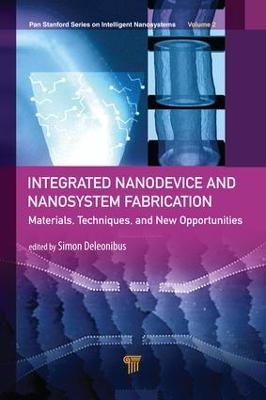
Integrated Nanodevice and Nanosystem Fabrication
Pan Stanford Publishing Pte Ltd (Verlag)
978-981-4774-22-2 (ISBN)
- Titel nicht im Sortiment
- Artikel merken
Integrated Nanodevice and Nanosystem Fabrication: Breakthroughs and Alternatives is the second volume in the Pan Stanford Series on Intelligent Nanosystems. The book contains 8 chapters and is divided into two parts, the first of which reports breakthrough materials and techniques such as single ion implantation in silicon and diamond, graphene and 2D materials, nanofabrication using scanning probe microscopes, while the second tackles the scaling and architectural aspects of silicon devices through HiK scaling for nanoCMOS, nanoscale epitaxial growth of group IV semiconductors, design for variability co-optimization in SOI FinFETs, and nanowires for CMOS and diversifications.
Simon Deleonibus retired from CEA-LETI on January 1, 2016, as chief scientist after 30 years of research on the architecture of micro- and nanoelectronic devices. Before joining CEA-LETI, he was with Thomson Semiconductors (1981-1986), where he developed and transferred to production advanced microelectronic devices and products. He obtained his PhD in applied physics from Paris University (1982). He is a visiting professor at the Tokyo Institute of Technology (Tokyo, Japan) since 2014, National Chiao Tung University (Hsinchu, Taiwan) since 2015, and the Chinese Academy of Science (Beijing, PRC) since 2016 . Prof. Deleonibus is distinguished research director of the CEA since 2002, distinguished lecturer at IEEE since 2004, fellow of the IEEE since 2006, and fellow of the Electrochemical Society since 2015. He was awarded the titles of Chevalier de l’Ordre National du Mérite (2004) and Chevalier de l’Ordre des Palmes Académiques (2011), as well as the 2005 Grand Prix de l’Académie des Technologies. He is a member of the ITRS since 1998, the European Research Council Panel since 2007, and the Nanosciences Foundation Board of Trustees since 2007. He was associate editor of the IEEE Transactions on Electron Devices (2008-2014) and a member of the IEEE Electron Devices Society Board of Governors (2009-2011 and 2012-2014), where he has been reelected for 2016-2018. Currently he is secretary of IEEE EDS (2016-2017) and chair of IEEE EDS Region 8 SRC (2015-2016).
Introduction: Will new materials, fabrication and architecture schemes emerge for CMOS survival?. Deterministic single-ion implantation method for quantum processing in silicon and diamond. Graphene and two-dimensional materials : extending silicon technology for the future? Nanofabrication using scanning probe microscopes. High-k dielectric scaling for nano CMOS technology. Nanometer scale epitaxial growth of group IV semiconductors. TCAD-based design technology co-optimization for variability in nanoscale SOI FinFETs. Nanowires for CMOS and diversifications.
| Erscheinungsdatum | 12.08.2017 |
|---|---|
| Reihe/Serie | Jenny Stanford Series on Intelligent Nanosystems |
| Zusatzinfo | 15 Tables, black and white; 10 Illustrations, color; 178 Illustrations, black and white |
| Verlagsort | Singapore |
| Sprache | englisch |
| Maße | 152 x 229 mm |
| Gewicht | 660 g |
| Themenwelt | Naturwissenschaften ► Physik / Astronomie ► Optik |
| Technik ► Elektrotechnik / Energietechnik | |
| Technik ► Maschinenbau | |
| ISBN-10 | 981-4774-22-7 / 9814774227 |
| ISBN-13 | 978-981-4774-22-2 / 9789814774222 |
| Zustand | Neuware |
| Informationen gemäß Produktsicherheitsverordnung (GPSR) | |
| Haben Sie eine Frage zum Produkt? |
aus dem Bereich


