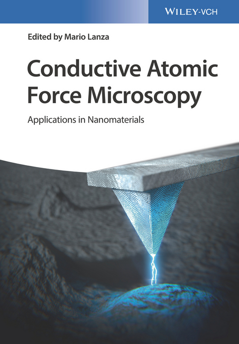
Conductive Atomic Force Microscopy
Wiley-VCH (Verlag)
978-3-527-34091-0 (ISBN)
Dr. Mario Lanza is a Young 1000 Talent Professor and group leader at the Institute of Functional Nano & Soft Materials, in Soochow University, China. He obtained his PhD in 2010 at the Electronic Engineering Department of Universitat Autonoma de Barcelona. In 2010 and 2011 he was postdoctoral scholar at Peking University in China, where he used the technique of conductive atomic force microscopy to characterize a wide range of two dimensional materials and nanowires. In 2012 and 2013 he was Marie Curie postdoctoral fellow at Stanford University, USA, where he used CAFM to study local defects in photoelectrodes for water-splitting solar cells. Dr. Lanza has published more than 60 publications, most of them using the CAFM to study the nanoelectronic properties of different materials and devices. Furthermore, he developed different setups to enhance the capabilities of the CAFM, including an environmental chamber and ultra durable graphene-coated probe tips. Currently his research group is focused on the nanoscale electrical characterization of different devices, including field effect transistors, non-volatile memories and solar cells.
Foreword
Preface
Introduction to CAFM: History, Experimental and Current Status
Reliability of Polycrystalline Thin Oxides and Insulators
Investigation of High-k Dielectric Stacks by TUNA and CAFM: Advantages, Limitations and Applications
3D Tomography for Analyzing Conductive Filaments for Resistive Random Access Memory Devices
CAFM Applications for Energy Efficient and High-Frequency Electronics
Local Anodic Oxidation with AFM Tips
CAFM Studies of Low-Dimensional Materials
Design of a Logarithmic Amplifier for CAFM
Resiscopes for Analyzing Wide Dynamic Current Ranges
Combination of CAFM with the Probestation for Characterization of Resistive Switching and Channel Hot Carriers Degradation in FETs
Multiprobe CAFM
Scanning Capacitance Microscopy as a Complementary Tool for CAFM
KPFM and its Use to Characterize the CPD in Different Materials
Hot-Electron Nanoscopy Using Adiabatic Compression of Surface Plasmons
Fabrication and Reliability of AFM Nanoprobes
| Erscheinungsdatum | 11.10.2017 |
|---|---|
| Verlagsort | Berlin |
| Sprache | englisch |
| Maße | 170 x 244 mm |
| Gewicht | 980 g |
| Themenwelt | Naturwissenschaften ► Chemie ► Analytische Chemie |
| Technik ► Elektrotechnik / Energietechnik | |
| Technik ► Maschinenbau | |
| Schlagworte | Chemie • Chemistry • Dünne Schichten, Oberflächen u. Grenzflächen • Electrical & Electronics Engineering • Electrical & Electronics Engineering • Electronic materials • Elektronische Materialien • Elektrotechnik u. Elektronik • Materials Science • Materialwissenschaften • Microscopy • Mikroskopie • Nanomaterial • Nanomaterialien • nanomaterials • Nanotechnologie • nanotechnology • Rasterkraftmikroskopie • Thin Films, Surfaces & Interfaces • Thin Films, Surfaces & Interfaces |
| ISBN-10 | 3-527-34091-2 / 3527340912 |
| ISBN-13 | 978-3-527-34091-0 / 9783527340910 |
| Zustand | Neuware |
| Haben Sie eine Frage zum Produkt? |
aus dem Bereich


