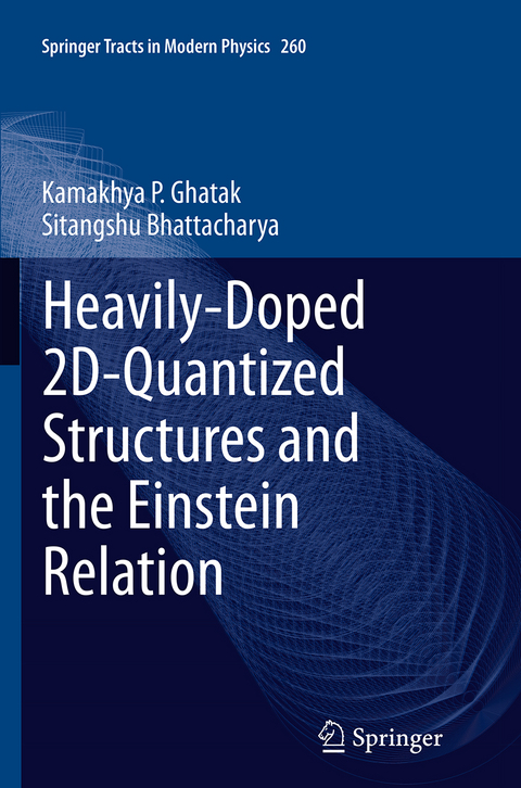
Heavily-Doped 2D-Quantized Structures and the Einstein Relation
Springer International Publishing (Verlag)
978-3-319-38127-5 (ISBN)
Born in India in 1953, Professor K. P. Ghatak obtained his B.E degree in Electronics and Telecommunication Branch from the then Bengal Engineering College Shibpur (Presently Bengal Engineering and Science University) of the University of Calcutta in 1974, M.Tech degree from the Institute of Radio Physics and Electronics of the University of Calcutta in 1976. He obtained his PhD (Tech) degree from the University of Calcutta in 1988 on the basis of 27 published research papers in International peer-reviewed Scientific Journals which is still a record in the said Institute. He joined as Lecturer in the Institute of Radio Physics and Electronics of the University of Calcutta in 1983, Reader in the Department of Electronics and Telecommunication Engineering of Jadavpur University in 1987 and Professor in the Department of Electronic Science of the University of Calcutta in 1994 and was at the top of the merit list in all the cases respectively. From March 2012, he has joined in the Department of Electronics and Communication Engineering of National Institute of Technology, Agartala, Tripura and presently acting as the Professor and Head of the said Department. Professor K. P. Ghatak is the First Recipient of the Degree of Doctor of Engineering of Jadavpur University in 1991 since the University inception in 1955 and in the same year he received the Indian National Science Academy visiting fellowship to IIT-Kharagpur. He is the principal co-author of more than 300 research papers on Semiconductor Nano-science in eminent peer-reviewed International Journals and more than 50 research papers in the Proceedings of SPIE and MRS and many of his papers are being cited many times. Professor Ghatak is the invited Speaker of SPIE, MRS, etc., the referee and Associate Editor of different eminent Journals. He has produced more than two dozens of PhD candidates in various aspects of materials and nano-sciences and many of them are working as Dean, Professor, Associate Professor and Assistant Professor in different Universities and reputed Academic Institutions. He is the principal co-author of the SIX research monographs entitled "Einstein Relation in Compound Semiconductors and Their Nanostructures" Springer Series in Materials Science, Vol. 116, 2009, which is the first monograph on Einstein relation containing more than 100 open research problems, "Photoemission from Optoelectronic materials and their nanostructures", Springer Series in Nano structure Science and Technology, USA in 2009 as the first monograph solely devoted to Photoemission from nano-structured compounds containing more than 100 open research problems, "Thermo electric power in nano structured materials: Strong magnetic fields" Springer Series in Materials Science Vol. 137, 2010 which is the first monograph on this topic containing 150 open research problems, "Fowler-Nordheim Field Emission : Effects in Semiconductor Nanostructures "Springer Series in Solid State Sciences, Vol. 170, 2012 which is the first monograph on this topic containing 200 open research problems, "Effective electron mass in low dimensional semiconductors" Springer Series in Materials Science Vol. 167, 2013 which is the first monograph on this pin pointed topic containing 250 open research problems and "Debye Screening Length: "Effects of nano-structured materials" which is the first book solely devoted to Debye Screening Length: Effects of Nano-structured Materials containing more than 100 open research problems which will published in Springer Tracts in Modern Physics in late 2013 respectively. He is the Principal Editor of the two edited monographs entitled "Bismuth:: Characteristics, Production and Applications: Series in Materials Science and Technologies" and "Quantum Dots and Quantum Cellular Automata: Recent Trends and Applications : Series in Nanotechnology Science" of NOVA , USA respectively. The All Indian Council for Technical Education has selected the first Research and Development projec
From the Contents: The ER in Quantum Wells (QWs) of Heavily Doped(HD) Non-Parabolic Semiconductors.- The ER in NIPI Structures of HD Non-Parabolic Semiconductors.- The ER in Accumulation Layers of HD Non-Parabolic Semiconductors.- Suggestion for Experimental Determinations of 2D and 3D ERs and few Related Applications.- Conclusion and Scope for Future.
| Erscheinungsdatum | 03.08.2016 |
|---|---|
| Reihe/Serie | Springer Tracts in Modern Physics |
| Zusatzinfo | XL, 347 p. 58 illus. |
| Verlagsort | Cham |
| Sprache | englisch |
| Maße | 155 x 235 mm |
| Themenwelt | Naturwissenschaften ► Chemie ► Analytische Chemie |
| Naturwissenschaften ► Physik / Astronomie ► Atom- / Kern- / Molekularphysik | |
| Naturwissenschaften ► Physik / Astronomie ► Festkörperphysik | |
| Schlagworte | 2D-quantized Structures • Einstein Relation in Semiconductors Under Strong E • Einstein Relation in Semiconductors Under Strong Electric Field • Einstein Relation in Super-lattices Under Magnetic • Einstein Relation in Super-lattices Under Magnetic Quantization • Electronic devices and materials • III-V, Ternary and Quaternary Semiconductors • Low-dimensional semiconductors • nanoscale science and technology • nanotechnology • Nanotechnology and Microengineering • optical and electronic materials • other manufacturing technologies • Physics and Astronomy • quantized optoelectronic semiconductors • Quantum Wells of Doped Non-parabolic Semiconductor • Quantum Wells of Doped Non-parabolic Semiconductors • semiconductors • Semiconductors Under External Photo-excitation • Solid state physics • Spectrum analysis, spectrochemistry, mass spectrom |
| ISBN-10 | 3-319-38127-X / 331938127X |
| ISBN-13 | 978-3-319-38127-5 / 9783319381275 |
| Zustand | Neuware |
| Informationen gemäß Produktsicherheitsverordnung (GPSR) | |
| Haben Sie eine Frage zum Produkt? |
aus dem Bereich


