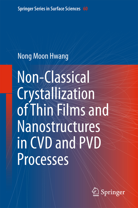
Non-Classical Crystallization of Thin Films and Nanostructures in CVD and PVD Processes (eBook)
XII, 332 Seiten
Springer Netherland (Verlag)
978-94-017-7616-5 (ISBN)
Prof. Hwang's research interest is in the microstructure evolutions during material processing, especially, abnormal grain growth and thin film growth. The topics are approached both experimentally and theoretically, occasionally using computer simulation. The most focused work has been the theory of charged clusters, which is suggested as a new understanding of thin film growth. This topic is related to the growth mechanism of thin films and nanowires, nanotubes prepared by chemical vapor deposition. The size distribution of charged clusters or nanoparticles is measured by differential mobility analyzer (DMA). He published more than 100 papers in SCI-indexed journals
This book provides a comprehensive introduction to a recently-developed approach to the growth mechanism of thin films and nanostructures via chemical vapour deposition (CVD). Starting from the underlying principles of the low pressure synthesis of diamond films, it is shown that diamond growth occurs not by individual atoms but by charged nanoparticles. This newly-discovered growth mechanism turns out to be general to many CVD and some physical vapor deposition (PVD) processes. This non-classical crystallization is a new paradigm of crystal growth, with active research taking place on growth in solution, especially in biomineralization processes. Established understanding of the growth of thin films and nanostructures is based around processes involving individual atoms or molecules. According to the author's research over the last two decades, however, the generation of charged gas phase nuclei is shown to be the rule rather than the exception in the CVD process, and charged gas phase nuclei are actively involved in the growth of films or nanostructures. This new understanding is called the theory of charged nanoparticles (TCN). This book describes how the non-classical crystallization mechanism can be applied to the growth of thin films and nanostructures in gas phase synthesis. Based on the author's graduate lecture course, the book is aimed at senior undergraduate and graduate students and researchers in the field of thin film and nanostructure growth or crystal growth. It is hoped that a new understanding of the growth processes of thin films and nanostructures will reduce trial-and-error in research and in industrial fabrication processes.
Prof. Hwang’s research interest is in the microstructure evolutions during material processing, especially, abnormal grain growth and thin film growth. The topics are approached both experimentally and theoretically, occasionally using computer simulation. The most focused work has been the theory of charged clusters, which is suggested as a new understanding of thin film growth. This topic is related to the growth mechanism of thin films and nanowires, nanotubes prepared by chemical vapor deposition. The size distribution of charged clusters or nanoparticles is measured by differential mobility analyzer (DMA). He published more than 100 papers in SCI-indexed journals
Preface 6
Contents 8
1 Non-classical Crystallization 14
1.1 Classical Versus Non-classical Crystallization 14
1.2 Theory of Charged Nanoparticles 17
1.3 Effect of Charge on the Bond Strength 18
1.4 Growth of Nanowires by Non-classical Crystallization 20
1.5 Direct Observation of Non-classical Crystallization 22
1.5.1 Growth of Pt3Fe Nanorods 22
1.5.2 Growth of Pt Crystals 25
1.6 Healing of Mg Nanopores by Electron Beam Irradiation 27
1.7 Particle Formation in the Chemical Vapour Deposition Process 29
References 30
2 Thermodynamics of Physical and Chemical Vapour Deposition 34
2.1 Ideal Gases 34
2.2 Driving Force for Evaporation 35
2.3 Driving Force for Condensation 37
2.4 Driving Force for Deposition in the Physical Vapour Deposition Process 37
2.5 Irreversibility for Chemical Reactions 38
2.6 Driving Force for Deposition in the Chemical Vapour Deposition Process 40
2.7 Consideration of the Substrate or Surface 44
2.8 Driving Force for Deposition of Compound or Solid Solution 44
2.9 Calculation Examples Using Thermo-Calc 46
2.9.1 Si–Cl–H System 46
2.9.2 Si–C–H System 47
2.10 Validity of the Thermodynamic Scheme 48
2.11 Maximum Film Growth Rate in the CVD Process 50
2.12 Driving Force for Deposition in the Diamond Chemical Vapour Deposition Process 50
2.13 Kinetics 61
References 62
3 Nucleation 64
3.1 Classical Nucleation Theory 64
3.2 Rate of Nucleation 66
3.3 Heterogeneous Nucleation 69
3.4 Preferential Nucleation Along Scratches on the Substrate in the Diamond CVD Process 75
3.5 Ion-Induced Nucleation: Heterogeneous Nucleation in the Gas Phase 77
3.6 Photo-Induced Nucleation: Heterogeneous Nucleation in the Gas Phase 82
References 83
4 Growth 85
4.1 Rough and Smooth Interfaces 85
4.2 Diffusion-Controlled Growth 86
4.3 Interface-Controlled Growth 88
4.3.1 Terrace-Ledge-Kink (TLK) Model 88
4.3.2 Growth by 2D Nucleation 90
4.3.3 Growth by Spiral Steps 93
4.3.4 Kinetic Roughening 94
4.3.5 Dissolution or Evaporation 95
4.4 Roughening Transition of the Interface 95
4.5 Equilibrium Shape 96
4.6 Growth Shape 97
4.7 Growth Shape of Diamond Crystals 98
4.8 Growth Mode and Morphology of Crystals 103
4.9 Secondary Nucleation on the Growing Interface 104
4.10 Nanocrystalline or Microcrystalline Grains Embedded in an Amorphous Matrix 106
4.11 Nanocrystalline Films 108
References 110
5 Diamond Synthesis at Low Pressure 112
5.1 High Pressure Synthesis of Diamond 112
5.2 Low Pressure Synthesis of Diamond (Old CVD Process) 113
5.2.1 Possibility of Gas Phase Nucleation in the Old CVD Diamond Process 114
5.3 Diamond Synthesis at Low Pressure (New CVD Process Using Gas Activation) 115
5.3.1 CVD Diamond Reactor and Processing Conditions 116
5.3.2 Phase Diagram of Carbon 117
5.4 Thermodynamics and Kinetics of the Diamond Synthesis at Low Pressure 118
5.5 Comparison of Stability Between Diamond and Graphite in the Nucleation Stage 120
5.6 Capillary Pressure of Diamond and Graphite in the Nucleation Stage 123
5.6.1 Relative Nucleation Rate of Diamond and Graphite 125
5.7 Diamonds in the Sky 127
5.8 Comparison of Nucleation Barrier Between Diamond and Graphite 129
5.9 Atomic Hydrogen Hypothesis 130
5.9.1 Distinction Between Reversible and Irreversible Fluxes 130
5.9.2 Criticism of Atomic Hydrogen Hypothesis 131
5.10 Diamond Deposition with Simultaneous Graphite Etching 133
5.11 Experimental Fact Appearing to Violate the Second Law of Thermodynamics 135
References 138
6 Growth Mechanism of CVD Diamond 142
6.1 Deposition Behaviour Between Silicon and Iron Substrates 142
6.2 Formation Mechanism of Soot 144
6.3 Preferential Formation of Soot at the Corner of Iron Substrates 145
6.4 Current Measurements in the CVD Diamond Reactor 145
6.5 Ion-Induced Nucleation 147
6.6 Which Property of Substrates Is Related with Soot Formation? 147
6.7 Comparison of Deposition Behaviour Between Floating and Grounded Iron Substrates 150
6.8 Charged Cluster Model 151
6.9 Experimental Verification of Hypothetical Diamond Nanoparticles in the Gas Phase 152
6.10 Experimental Evidences for Diamond Etching During the CVD Diamond Process 156
6.11 Ex-situ Observation of Diamond Clusters 157
6.12 Effect of Methane Concentration on the Size of Charged Clusters 160
6.13 Diamond Synthesis Without Hydrogen at Low Pressure 163
6.14 Growth Rate With and Without Gas Phase Nucleation 165
6.15 Deposition Behaviour of Charged Clusters 166
6.15.1 Preferential Diamond Formation on the Edge 166
6.15.2 Bias Effect in the Hot Filament CVD Process 167
6.15.3 Bias Effect in the DC Plasma Process 168
6.15.4 Bias Enhanced Nucleation (BEN) 169
References 169
7 Growth Mechanism of CVD Silicon 174
7.1 Simultaneous Deposition and Etching of Silicon During CVD 174
7.2 Deposition Behaviour Between Conducting, Semi-conducting and Insulating Substrates 180
7.3 Deposition Behaviour on Substrates with Different Charge Transfer Rates 184
7.4 Growth of Silicon Nanowires 186
References 190
8 Other Works Related to Non-classical Crystallization of Thin Films and Nanostructures 192
8.1 Hot Cluster Epitaxy by Thermal Plasma Flash Evaporation 192
8.2 Polymorphous Si Films by Plasma Enhanced CVD 195
8.3 Nano-Fabrications Using the Building Blocks Generated in Plasma 199
References 200
9 Experimental Confirmation of Charged Nanoparticles During Atmospheric CVD Using Differential Mobility Analyser 203
9.1 Differential Mobility Analyzer and Faraday Cup Electrometer 203
9.2 Generation of Charged Nanoparticles During the Synthesis of ZnO Nanostructures 207
9.2.1 In-situ Measurements of CNPs by DMA During the Synthesis of ZnO Nanostructures 207
9.2.2 Formation Mechanism of Charged Nanoparticles 209
9.3 Generation of Charged Nanoparticles During the Synthesis of Carbon Nanotubes 210
9.3.1 Hot Filament CVD Process 211
9.3.2 Measurements of CNPs by DMA During Atmospheric CVD 214
9.4 Generation of Charged Nanoparticles During the Synthesis of Si Films 218
9.5 Generation of Charged Nanoparticles During the Synthesis of Si Nanowires 220
9.6 Generation of Charged Nanoparticles During the Synthesis of GaN Nanostructures 224
References 229
10 Experimental Confirmation of Charged Nanoparticles at Low Pressure 233
10.1 Measurements of Nanoparticles Using a Low Pressure Differential Mobility Analyser 233
10.2 Measurements of Particle Size in Plasma Enhanced CVD Using a Low Pressure Differential Mobility Analyzer 235
10.3 Measurements of Particle Size During Laser Ablation Using a Low Pressure Differential Mobility Analyzer 237
10.4 Measurements of CNPs During Si Hot Wire CVD Using a Particle Beam Mass Spectrometer 239
References 248
11 Deposition Behavior of Charged Nanoparticles 250
11.1 Comparison of Deposition Behavior of Si Between Floating and Grounded Substrates 250
11.2 Evolution of Puzzling Microstructures During Si CVD 254
11.3 Growth of Silicon Nanostructures by Thermal Evaporation of SiO Powders 262
11.4 Various ZnO Nanostructures 264
References 268
12 Bias Effect on Deposition Behaviour of Charged Nanoparticles 269
12.1 Dependence of Bias Effect on the Conductivity of Depositing Materials and Substrates 269
12.2 Bias Effect on Deposition Behavior of Si on Conducting, Insulating and Semiconducting Substrates 270
12.3 Comparison of Charge Generation from Hot Wires Between AC and DC Power Supply 277
12.3.1 Comparison of the Effect of Wire Bias Between AC and DC Powers 280
12.4 Non-uniform Deposition Using AC Power Supply in Si HWCVD 281
12.5 Effect of Alternating Bias on Deposition in Si CVD 285
12.6 Effect of Alternating Bias During ZnO CVD 290
References 296
13 Charge-Enhanced Kinetics 298
13.1 Magic Size 298
13.2 Experimental Evidences of Charge-Enhanced Diffusion During In-situ TEM Observation 300
13.2.1 Au Nanoparticles Under Electron-Beam Irradiation 301
13.2.2 Melting Point Depression 303
13.2.3 Electron-Assisted Superplasticity of Amorphous Silica 304
13.3 Comparison of Deposition Behaviour Between Neutral and Charged Nanoparticles 305
13.4 Gas-Mediated Electron or Ion Beam Induced Deposition and Etching 308
13.5 Catalytic Effect by Charge 311
References 312
14 Implications and Applications 314
14.1 Summary of the Theory of Charged Nanoparticles 314
14.2 Implications in Thin Film Processes 315
14.2.1 CVD Process 315
14.2.2 Plasma Enhanced CVD (PECVD) 316
14.2.3 Low Pressure Synthesis of Diamonds 316
14.2.4 Conducting and Insulating CNPs 317
14.2.5 Thermal Evaporation 317
14.2.6 Sputtering 320
14.2.7 Pulsed Laser Ablation 321
14.2.8 Aerosol Deposition 321
14.2.9 Aerosol CVD 322
14.2.10 Electrospray Deposition 322
14.3 Applications in the CVD Process 323
14.3.1 Epitaxial and Non-epitaxial Growth 323
14.3.2 Low Temperature Deposition of Crystalline Phase 324
14.3.3 Amorphous Incubation Layer 326
14.4 Phenomena that Might Be Related with Charge-Enhanced Diffusion 333
References 333
Index 337
| Erscheint lt. Verlag | 14.6.2016 |
|---|---|
| Reihe/Serie | Springer Series in Surface Sciences | Springer Series in Surface Sciences |
| Zusatzinfo | XII, 332 p. 229 illus., 64 illus. in color. |
| Verlagsort | Dordrecht |
| Sprache | englisch |
| Themenwelt | Naturwissenschaften ► Physik / Astronomie ► Atom- / Kern- / Molekularphysik |
| Naturwissenschaften ► Physik / Astronomie ► Festkörperphysik | |
| Naturwissenschaften ► Physik / Astronomie ► Theoretische Physik | |
| Technik ► Elektrotechnik / Energietechnik | |
| Technik ► Maschinenbau | |
| Schlagworte | Chemical vapor deposition • Colloidal Crystallization • CVD Phase Diagram • Diamond Deposition • Driving Force for Deposition • Electrically Floated Silicon Substrate • Electrostatic Energy • Gas Flow Dynamics • Gas Phase Nuclei • Graphite Substrate • Heterogeneous nucleation • Homogeneous Nucleation • Metastable Diamond • Nano-sized Voids • Nanowires • Self-Assembly • Theory of Charged Nanoparticles • Thermodynamic Paradox • Void-free Dense Films |
| ISBN-10 | 94-017-7616-4 / 9401776164 |
| ISBN-13 | 978-94-017-7616-5 / 9789401776165 |
| Informationen gemäß Produktsicherheitsverordnung (GPSR) | |
| Haben Sie eine Frage zum Produkt? |
DRM: Digitales Wasserzeichen
Dieses eBook enthält ein digitales Wasserzeichen und ist damit für Sie personalisiert. Bei einer missbräuchlichen Weitergabe des eBooks an Dritte ist eine Rückverfolgung an die Quelle möglich.
Dateiformat: PDF (Portable Document Format)
Mit einem festen Seitenlayout eignet sich die PDF besonders für Fachbücher mit Spalten, Tabellen und Abbildungen. Eine PDF kann auf fast allen Geräten angezeigt werden, ist aber für kleine Displays (Smartphone, eReader) nur eingeschränkt geeignet.
Systemvoraussetzungen:
PC/Mac: Mit einem PC oder Mac können Sie dieses eBook lesen. Sie benötigen dafür einen PDF-Viewer - z.B. den Adobe Reader oder Adobe Digital Editions.
eReader: Dieses eBook kann mit (fast) allen eBook-Readern gelesen werden. Mit dem amazon-Kindle ist es aber nicht kompatibel.
Smartphone/Tablet: Egal ob Apple oder Android, dieses eBook können Sie lesen. Sie benötigen dafür einen PDF-Viewer - z.B. die kostenlose Adobe Digital Editions-App.
Buying eBooks from abroad
For tax law reasons we can sell eBooks just within Germany and Switzerland. Regrettably we cannot fulfill eBook-orders from other countries.
aus dem Bereich


