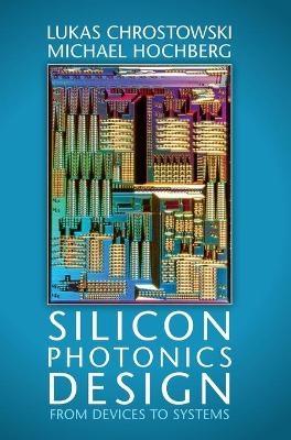
Silicon Photonics Design
Cambridge University Press (Verlag)
978-1-107-08545-9 (ISBN)
From design and simulation through to testing and fabrication, this hands-on introduction to silicon photonics engineering equips students with everything they need to begin creating foundry-ready designs. In-depth discussion of real-world issues and fabrication challenges ensures that students are fully equipped for careers in industry. Step-by-step tutorials, straightforward examples, and illustrative source code fragments guide students through every aspect of the design process, providing a practical framework for developing and refining key skills. Offering industry-ready expertise, the text supports existing PDKs for CMOS UV-lithography foundry services (OpSIS, ePIXfab, imec, LETI, IME and CMC) and the development of new kits for proprietary processes and clean-room based research. Accompanied by additional online resources to support students, this is the perfect learning package for senior undergraduate and graduate students studying silicon photonics design, and academic and industrial researchers involved in the development and manufacture of new silicon photonics systems.
Lukas Chrostowski is Associate Professor of Electrical and Computer Engineering at the University of British Columbia. He is the Program Director of the NSERC CREATE Silicon Electronic-Photonic Integrated Circuits (Si-EPIC) training program, has been teaching silicon photonics courses and workshops since 2008, and has been awarded the Killiam Teaching Prize (2014). Michael Hochberg is Director of Architecture and Strategy for Coriant Advanced Technology Group, based in Manhattan, New York, where he holds a visiting appointment at Columbia University. He has held faculty positions at the University of Washington, University of Delaware and National University of Singapore, and was Director of the OpSIS foundry-access service. He has co-founded several startups, including Simulant and Luxtera and received a Presidential Early Career Award in Science and Engineering (2009).
Part I. Silicon Photonics - Introduction: 1. Fabless Silicon Photonics: 1.1 Introduction; 1.2 Silicon photonics - the next fabless semiconductor industry; 1.3 Applications; 1.4 Technical challenges and the state of the art; 1.5 Opportunities; 2. Modelling and Design Approaches: 2.1 Optical Waveguide Mode Solver; 2.2 Wave Propagation; 2.3 Optoelectronic models; 2.4 Microwave Modelling; 2.5 Thermal Modelling; 2.6 Photonic Circuit Modelling; 2.7 Physical Layout; 2.8 Software Tools Integration; Part II. Silicon Photonics - Passive Components: 3. Optical Materials and Waveguides: 3.1 Silicon-on-Insulator; 3.2 Waveguides; 3.3 Bent waveguides; 3.4 Code Listings; 3.5 Problems; 4. Fundamental Building Blocks: 4.1 Directional couplers; 4.2 Y-Branch; 4.3 Mach-Zehnder Interferometer; 4.4 Ring resonators; 4.5 Waveguide Bragg Grating Filters; 4.6 Code Listings; 4.7 Problems; 5. Optical I/O: 5.1 The challenge of optical coupling to silicon photonic chips; 5.2 Grating Coupler; 5.3 Edge Coupler; 5.4 Polarization; 5.5 Code Listings; 5.6 Problems; Part III. Silicon Photonics - Active Components: 6. Modulators: 6.1 Plasma Dispersion E; 6.2 PN Junction Phase Shifter; 6.3 Micro-ring Modulators; 6.4 Forward-biased PIN Junction; 6.5 Active Tuning; 6.6 Thermo-Optic Switch; 6.7 Code Listings; 6.8 Problems; 7. Detectors: 7.1 Performance Parameters; 7.2 Fabrication; 7.3 Types of detectors; 7.4 Design Considerations; 7.5 Detector modelling; 7.5.2 Electronic Simulations; 7.6 Code Listings; 7.7 Problems; 8. Lasers: 8.1 External Lasers; 8.2 Laser Modelling; 8.3 Co-Packaging; 8.4 Hybrid Silicon Lasers; 8.5 Monolithic Lasers; 8.6 Alternative Light Sources; 8.7 Problems; Part IV. Silicon Photonics - System Design: 9. Photonic Circuit Modelling: 9.1 Need for photonic circuit modelling; 9.2 Components for System Design; 9.3 Compact Models; 9.4 Directional Coupler - Compact Model; 9.5 Ring Modulator - Circuit Model; 9.6 Grating Coupler - S Parameters; 9.7 Code Listings; 10. Tools and Techniques: 10.1 Process Design Kit (PDK); 10.2 Mask Layout; 11. Fabrication: 11.1 Fabrication Non-Uniformity; 11.2 Problems; 12. Testing and Packaging: 12.1 Electrical and Optical Interfacing; 12.2 Automated Optical Probe Stations; 12.3 Design for Test; 13. Silicon Photonic System Example: 13.1 Wavelength Division Multiplexed Transmitter.
| Zusatzinfo | 130 Halftones, color; 120 Line drawings, color |
|---|---|
| Verlagsort | Cambridge |
| Sprache | englisch |
| Maße | 182 x 256 mm |
| Gewicht | 1020 g |
| Themenwelt | Naturwissenschaften ► Physik / Astronomie ► Optik |
| Technik ► Elektrotechnik / Energietechnik | |
| ISBN-10 | 1-107-08545-4 / 1107085454 |
| ISBN-13 | 978-1-107-08545-9 / 9781107085459 |
| Zustand | Neuware |
| Haben Sie eine Frage zum Produkt? |
aus dem Bereich


