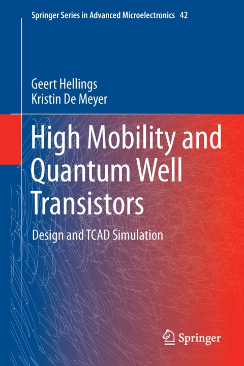
High Mobility and Quantum Well Transistors (eBook)
XVIII, 140 Seiten
Springer Netherlands (Verlag)
978-94-007-6340-1 (ISBN)
High Mobility and Quantum Well Transistors: Design and TCAD Simulation investigates planar bulk Germanium pFET technology in chapters 2-4, focusing on both the fabrication of such a technology and on the process and electrical TCAD simulation. Furthermore, this book shows that Quantum Well based transistors can leverage the benefits of these alternative materials, since they confine the charge carriers to the high-mobility material using a heterostructure. The design and fabrication of one particular transistor structure - the SiGe Implant-Free Quantum Well pFET - is discussed. Electrical testing shows remarkable short-channel performance and prototypes are found to be competitive with a state-of-the-art planar strained-silicon technology. High mobility channels, providing high drive current, and heterostructure confinement, providing good short-channel control, make a promising combination for future technology nodes.
Geert Hellings received the B.S. and M.S. degrees in Electrical Engineering from the KU Leuven, Belgium, in 2007. His master thesis was on III-nitride-based UV detectors for space applications. He obtained the PhD degree from the Electrical Engineering Department (ESAT), Integrated Systems Division (INSYS) at the University of Leuven, Belgium. During his PhD, he worked on the integration of high-mobility channel materials for digital logic applications at imec, Leuven, Belgium. He received a Ph.D. grant from the Institute for the Promotion of Innovation through Science and Technology in Flanders (IWT-Vlaanderen), Brussels, Belgium. He won the 2008 IEEE Region 8 Student Paper Contest and received the 2011 imec Scientific Excellence Award. He has authored or co-authored approximately 70 technical papers for publication in journals and presentations at conferences and holds various patents.
Kristin De Meyer M.Sc. (1974), PhD (1979) KULeuven. She was holder of an IBM World Trade Postdoctoral Fellowship at the IBM T. J. Watson Research Center, Yorktown Heights, NY. Currently she is the Director of Doctoral Research in imec. Since October 1986, she has also been a Part-Time Professor with ESAT-INSYS, KUL. She was the Coordinator for IMEC in several EEC projects. Dr. De Meyer is an IIEE fellow ,member of the Belgian Federal Council for Science Policy and (co) author of over 500 publications.
For many decades, the semiconductor industry has miniaturized transistors, delivering increased computing power to consumers at decreased cost. However, mere transistor downsizing does no longer provide the same improvements. One interesting option to further improve transistor characteristics is to use high mobility materials such as germanium and III-V materials. However, transistors have to be redesigned in order to fully benefit from these alternative materials.High Mobility and Quantum Well Transistors: Design and TCAD Simulation investigates planar bulk Germanium pFET technology in chapters 2-4, focusing on both the fabrication of such a technology and on the process and electrical TCAD simulation. Furthermore, this book shows that Quantum Well based transistors can leverage the benefits of these alternative materials, since they confine the charge carriers to the high-mobility material using a heterostructure. The design and fabrication of one particular transistor structure - the SiGe Implant-Free Quantum Well pFET - is discussed. Electrical testing shows remarkable short-channel performance and prototypes are found to be competitive with a state-of-the-art planar strained-silicon technology. High mobility channels, providing high drive current, and heterostructure confinement, providing good short-channel control, make a promising combination for future technology nodes.
Geert Hellings received the B.S. and M.S. degrees in Electrical Engineering from the KU Leuven, Belgium, in 2007. His master thesis was on III-nitride-based UV detectors for space applications. He obtained the PhD degree from the Electrical Engineering Department (ESAT), Integrated Systems Division (INSYS) at the University of Leuven, Belgium. During his PhD, he worked on the integration of high-mobility channel materials for digital logic applications at imec, Leuven, Belgium. He received a Ph.D. grant from the Institute for the Promotion of Innovation through Science and Technology in Flanders (IWT-Vlaanderen), Brussels, Belgium. He won the 2008 IEEE Region 8 Student Paper Contest and received the 2011 imec Scientific Excellence Award. He has authored or co-authored approximately 70 technical papers for publication in journals and presentations at conferences and holds various patents. Kristin De Meyer M.Sc. (1974), PhD (1979) KULeuven. She was holder of an IBM World Trade Postdoctoral Fellowship at the IBM T. J. Watson Research Center, Yorktown Heights, NY. Currently she is the Director of Doctoral Research in imec. Since October 1986, she has also been a Part-Time Professor with ESAT-INSYS, KUL. She was the Coordinator for IMEC in several EEC projects. Dr. De Meyer is an IIEE fellow ,member of the Belgian Federal Council for Science Policy and (co) author of over 500 publications.
List of Abbreviations and Symbols. 1 Introduction. 1.1 Transistor Scaling. 1.2 What’s Next? (2010 - ...). 1.3 Goals of the Book. 1.4 Organization of the Book. 2 S/D Junctions in Ge: experimental. 2.1 Introduction. 2.2 P-type Junctions. 2.3 N-Type Junctions. 2.4 Benchmarking. 2.5 Summary and Conclusions. 3 TCAD Simulation and Modeling of Ion Implants in Germanium. 3.1 Introduction. 3.2 Ion Implant into Germanium - Monte Carlo Simulations. 3.3 Ion Implant into Germanium - Analytical Description. 3.4 Application to a 70 nm Bulk Ge pFET Technology. 3.5 Summary and Conclusions. 4 Electrical TCAD Simulations and Modeling in Germanium. 4.1 Introduction. 4.2 TCAD Models for a Germanium pMOSFET technology. 4.3 Electrical TCAD simulations - 65 nm Ge pMOSFET Technology. 4.4 Impact of Interface Traps MOS Performance. 4.5 Summary and Conclusions. 5 Investigation of Quantum Well Transistors for Scaled Technologies. 5.1 Introduction. 5.2 Motivation - Scalability Issues in Bulk MOSFET Technologies. 5.3 Towards A Scalable Transistor Architecture. 5.4 High Electron Mobility Transistors: an Alternative Approach. 5.5 Operation of Heterostructure Transistors: Analytical Description. 5.6 Conclusions. 6 Implant-Free Quantum Well FETs: Experimental investigation. 6.1 Introduction. 6.2 First-Generation SiGe Implant-Free Quantum Well pFET. 6.3 Enhancing Performance in SiGe IFQW pFETs. 6.4 Second-generation Strained SiGe IFQW pFETs. 6.5 Matching Performance and VT -Tuning in IFQW pFETs. 6.6 SiGe Quantum Well Diffusion Study. 6.7 Conclusions. 7 Conclusions Future Work and Outlook. 7.1 Conclusions. 7.2 Future Work and Outlook. Bibliography. List of Publications.
| Erscheint lt. Verlag | 25.3.2013 |
|---|---|
| Reihe/Serie | Springer Series in Advanced Microelectronics |
| Zusatzinfo | XVIII, 140 p. |
| Verlagsort | Dordrecht |
| Sprache | englisch |
| Themenwelt | Naturwissenschaften ► Physik / Astronomie |
| Technik ► Elektrotechnik / Energietechnik | |
| Technik ► Maschinenbau | |
| Schlagworte | Drain Junction • FETs • High-mobility semiconductors • Implant-Free • Ion Implants in Germanium • Quantum Well Transistors • Scaled Technologies • Silicon Germanium • TCAD Modeling • TCAD Simulation |
| ISBN-10 | 94-007-6340-9 / 9400763409 |
| ISBN-13 | 978-94-007-6340-1 / 9789400763401 |
| Haben Sie eine Frage zum Produkt? |
Größe: 4,8 MB
DRM: Digitales Wasserzeichen
Dieses eBook enthält ein digitales Wasserzeichen und ist damit für Sie personalisiert. Bei einer missbräuchlichen Weitergabe des eBooks an Dritte ist eine Rückverfolgung an die Quelle möglich.
Dateiformat: PDF (Portable Document Format)
Mit einem festen Seitenlayout eignet sich die PDF besonders für Fachbücher mit Spalten, Tabellen und Abbildungen. Eine PDF kann auf fast allen Geräten angezeigt werden, ist aber für kleine Displays (Smartphone, eReader) nur eingeschränkt geeignet.
Systemvoraussetzungen:
PC/Mac: Mit einem PC oder Mac können Sie dieses eBook lesen. Sie benötigen dafür einen PDF-Viewer - z.B. den Adobe Reader oder Adobe Digital Editions.
eReader: Dieses eBook kann mit (fast) allen eBook-Readern gelesen werden. Mit dem amazon-Kindle ist es aber nicht kompatibel.
Smartphone/Tablet: Egal ob Apple oder Android, dieses eBook können Sie lesen. Sie benötigen dafür einen PDF-Viewer - z.B. die kostenlose Adobe Digital Editions-App.
Zusätzliches Feature: Online Lesen
Dieses eBook können Sie zusätzlich zum Download auch online im Webbrowser lesen.
Buying eBooks from abroad
For tax law reasons we can sell eBooks just within Germany and Switzerland. Regrettably we cannot fulfill eBook-orders from other countries.
aus dem Bereich


