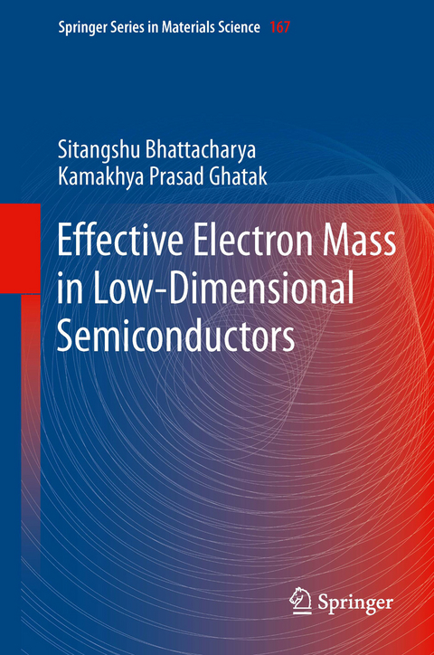
Effective Electron Mass in Low-Dimensional Semiconductors (eBook)
XXIV, 536 Seiten
Springer Berlin (Verlag)
978-3-642-31248-9 (ISBN)
The book is written for post graduate students, researchers and engineers, professionals in the fields of solid state sciences, materials science, nanoscience and technology, nanostructured materials and condensed matter physics.
Dr. S. Bhattacharya obtained his M. Sc. and Ph.D Degree from Electronic Science of the University of Calcutta and Jadavpur University, India in 2003 and 2009 respectively and is presently working at the Centre for Electronics Design and Technology, Indian Institute of Science, Bangalore. His current work involves the investigations of transport properties of different nanoscaled materials and devices under various external conditions. He is the co-author of more than 50 scientific research papers in different aspects of nanostructures in international peer-reviewed journals of high repute. He is also the co-author of the FOUR research monographs entitled 'Einstein Relation in Compound Semiconductors and Their Nanostructures' Springer Series in Materials Science, Vol. 116,2009 which is the first book on Einstein relation and contains more than 100 open research problems, 'Photoemission from Optoelectronic materials and their nanostructures',Springer Series in Nano structure Science and Technology, USA in 2009 as the first book solely devoted to Photoemission from nanostructured optoelectronic materials and contents more than 100 open research problems, 'Thermo electric power in nano structured materials under strong magnetic field' Springer Series in Materials Science Vol. 137 ,2010 and contents one hundred and fifty open research problems and 'Fowler-Nordheim Field Emission from Semiconductor Nanostructures' Springer Series in Solid State Sciences, Vol. 170, 2011 which is the first book on Fowler-Nordheim Field Emission containing 200 open research problems respectively. His present research interests are the quantum effect devices and nonlinearities. Besides, he is an invited speaker in different reputed International Conferences on nanoscale systems and devices.
Born in India in 1953.Professor K. P. Ghatak obtained his B.E degree in Electronics and Telecommunication Engineering in 1974 from the then Bengal Engineering college Shibpur(Presently Bengal Engineering and Science University) in 1974, M.Tech and PhD(Tech) degrees from the Institute of Radio Physics and Electronics of The University of Calcutta in 1976 and 1988 respectively.He joined as Lecturer in the Institute of Radio Physics and Electronics of the University of Calcutta in 1983, Reader in the Department of Electronics and Telecommunication of Jadavpur University in 1987 and Professor in the Department of Electronic Science of the University of Calcutta in 1994 and was at the top of the merit list in all the cases respectively. Professor K. P. Ghatak is the First Recipient of the Degree of Doctor of Engineering of Jadavpur University in 1991 since the University inception in 1955 and in the same year he received the Indian National Science Academy visiting fellowship to IIT-Kharagpur. His present research interests are nano science and number thoery. He is the principal co-author of more than 200 research papers on Semiconductor and Nanoscience in eminent peer-reviewed International Journals and more than 50 research papers in the Proceedings of the International Conferences held in USA and many of his papers are being cited many times. Professor Ghatak is the invited Speaker of SPIE, MRS, etc. and is the referee of different eminent Journals. He is the supervisor of more than two dozens of Ph.D candidates in various aspects of materials and nanoscience and many of them are working as Professor, Associate Professor and Assistant Professor in different Universities and reputed Academic Institutions. He is the principal co-author of the said FOUR research monographs. The All Indian Council For Technical Education has selected the first Research and Development project in his life for the best project award in Electronics and second best research project award considering all the branches of Engineering for the year 2006.
Dr. S. Bhattacharya obtained his M. Sc. and Ph.D Degree from Electronic Science of the University of Calcutta and Jadavpur University, India in 2003 and 2009 respectively and is presently working at the Centre for Electronics Design and Technology, Indian Institute of Science, Bangalore. His current work involves the investigations of transport properties of different nanoscaled materials and devices under various external conditions. He is the co-author of more than 50 scientific research papers in different aspects of nanostructures in international peer-reviewed journals of high repute. He is also the co-author of the FOUR research monographs entitled "Einstein Relation in Compound Semiconductors and Their Nanostructures" Springer Series in Materials Science, Vol. 116,2009 which is the first book on Einstein relation and contains more than 100 open research problems, "Photoemission from Optoelectronic materials and their nanostructures",Springer Series in Nano structure Science and Technology, USA in 2009 as the first book solely devoted to Photoemission from nanostructured optoelectronic materials and contents more than 100 open research problems, "Thermo electric power in nano structured materials under strong magnetic field" Springer Series in Materials Science Vol. 137 ,2010 and contents one hundred and fifty open research problems and "Fowler-Nordheim Field Emission from Semiconductor Nanostructures" Springer Series in Solid State Sciences, Vol. 170, 2011 which is the first book on Fowler-Nordheim Field Emission containing 200 open research problems respectively. His present research interests are the quantum effect devices and nonlinearities. Besides, he is an invited speaker in different reputed International Conferences on nanoscale systems and devices. Born in India in 1953.Professor K. P. Ghatak obtained his B.E degree in Electronics and Telecommunication Engineering in 1974 from the then Bengal Engineering college Shibpur(Presently Bengal Engineering and Science University) in 1974, M.Tech and PhD(Tech) degrees from the Institute of Radio Physics and Electronics of The University of Calcutta in 1976 and 1988 respectively.He joined as Lecturer in the Institute of Radio Physics and Electronics of the University of Calcutta in 1983, Reader in the Department of Electronics and Telecommunication of Jadavpur University in 1987 and Professor in the Department of Electronic Science of the University of Calcutta in 1994 and was at the top of the merit list in all the cases respectively. Professor K. P. Ghatak is the First Recipient of the Degree of Doctor of Engineering of Jadavpur University in 1991 since the University inception in 1955 and in the same year he received the Indian National Science Academy visiting fellowship to IIT-Kharagpur. His present research interests are nano science and number thoery. He is the principal co-author of more than 200 research papers on Semiconductor and Nanoscience in eminent peer-reviewed International Journals and more than 50 research papers in the Proceedings of the International Conferences held in USA and many of his papers are being cited many times. Professor Ghatak is the invited Speaker of SPIE, MRS, etc. and is the referee of different eminent Journals. He is the supervisor of more than two dozens of Ph.D candidates in various aspects of materials and nanoscience and many of them are working as Professor, Associate Professor and Assistant Professor in different Universities and reputed Academic Institutions. He is the principal co-author of the said FOUR research monographs. The All Indian Council For Technical Education has selected the first Research and Development project in his life for the best project award in Electronics and second best research project award considering all the branches of Engineering for the year 2006.
Part I: Influence of Light Waves on the Effective Electron Mass (EEM) in Optoelectronic Semiconductors.- Part II: Influence of Quantum Confinement on the EEM in Non-Parabolic Semiconductors.- Part III: The EEM in Quantum Confined Superlattices of Non- Parabolic Semiconductors.- Part IV: Influence of Intense Electric Field on the EEM in Optoelectronic Semiconductors.
| Erscheint lt. Verlag | 5.10.2012 |
|---|---|
| Reihe/Serie | Springer Series in Materials Science | Springer Series in Materials Science |
| Zusatzinfo | XXIV, 536 p. |
| Verlagsort | Berlin |
| Sprache | englisch |
| Themenwelt | Naturwissenschaften ► Physik / Astronomie ► Atom- / Kern- / Molekularphysik |
| Technik ► Maschinenbau | |
| Schlagworte | EEM book • EEM review • effective electron mass, EEM • Low dimensional semiconductors • non-parabolic Semiconductors • optoelectronic Semiconductors • quantized optoelectronic semiconductors • quantum confined materials • quantum wells, wires, superlattices • Quantum Wires |
| ISBN-10 | 3-642-31248-9 / 3642312489 |
| ISBN-13 | 978-3-642-31248-9 / 9783642312489 |
| Haben Sie eine Frage zum Produkt? |
Größe: 12,4 MB
DRM: Digitales Wasserzeichen
Dieses eBook enthält ein digitales Wasserzeichen und ist damit für Sie personalisiert. Bei einer missbräuchlichen Weitergabe des eBooks an Dritte ist eine Rückverfolgung an die Quelle möglich.
Dateiformat: PDF (Portable Document Format)
Mit einem festen Seitenlayout eignet sich die PDF besonders für Fachbücher mit Spalten, Tabellen und Abbildungen. Eine PDF kann auf fast allen Geräten angezeigt werden, ist aber für kleine Displays (Smartphone, eReader) nur eingeschränkt geeignet.
Systemvoraussetzungen:
PC/Mac: Mit einem PC oder Mac können Sie dieses eBook lesen. Sie benötigen dafür einen PDF-Viewer - z.B. den Adobe Reader oder Adobe Digital Editions.
eReader: Dieses eBook kann mit (fast) allen eBook-Readern gelesen werden. Mit dem amazon-Kindle ist es aber nicht kompatibel.
Smartphone/Tablet: Egal ob Apple oder Android, dieses eBook können Sie lesen. Sie benötigen dafür einen PDF-Viewer - z.B. die kostenlose Adobe Digital Editions-App.
Zusätzliches Feature: Online Lesen
Dieses eBook können Sie zusätzlich zum Download auch online im Webbrowser lesen.
Buying eBooks from abroad
For tax law reasons we can sell eBooks just within Germany and Switzerland. Regrettably we cannot fulfill eBook-orders from other countries.
aus dem Bereich


