Chips 2020 (eBook)
XXVIII, 477 Seiten
Springer Berlin (Verlag)
978-3-642-23096-7 (ISBN)
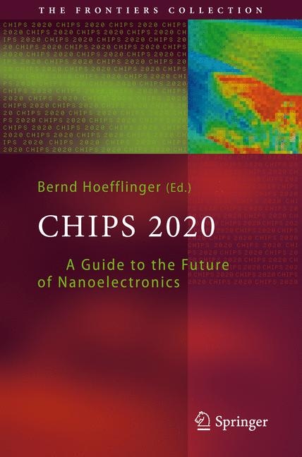
The chips in present-day cell phones already contain billions of sub-100-nanometer transistors. By 2020, however, we will see systems-on-chips with trillions of 10-nanometer transistors. But this will be the end of the miniaturization, because yet smaller transistors, containing just a few control atoms, are subject to statistical fluctuations and thus no longer useful. We also need to worry about a potential energy crisis, because in less than five years from now, with current chip technology, the internet alone would consume the total global electrical power!
This book presents a new, sustainable roadmap towards ultra-low-energy (femto-Joule), high-performance electronics. The focus is on the energy-efficiency of the various chip functions: sensing, processing, and communication, in a top-down spirit involving new architectures such as silicon brains, ultra-low-voltage circuits, energy harvesting, and 3D silicon technologies. Recognized world leaders from industry and from the research community share their views of this nanoelectronics future. They discuss, among other things, ubiquitous communication based on mobile companions, health and care supported by autonomous implants and by personal carebots, safe and efficient mobility assisted by co-pilots equipped with intelligent micro-electromechanical systems, and internet-based education for a billion people from kindergarden to retirement. This book should help and interest all those who will have to make decisions associated with future electronics: students, graduates, educators, and researchers, as well as managers, investors, and policy makers.
Introduction: Towards Sustainable 2020 Nanoelectronics.- From Microelectronics to Nanoelectronics.- The Future of Eight Chip Technologies.- Analog-Digital Interfaces.- Interconnects and Transceivers.- Requirements and Markets for Nanoelectronics.- ITRS: The International Technology Roadmap for Semiconductors.- Nanolithography.- Power-Efficient Design Challenges.- Superprocessors and Supercomputers.- Towards Terabit Memories.- 3D Integration for Wireless Multimedia.- The Next-Generation Mobile User-Experience.- MEMS (Micro-Electro-Mechanical Systems) for Automotive and Consumer.- Vision Sensors and Cameras.- Digital Neural Networks for New Media.- Retinal Implants for Blind Patients.- Silicon Brains.- Energy Harvesting and Chip Autonomy.- The Energy Crisis.- The Extreme-Technology Industry.- Education and Research for the Age of Nanoelectronics.- 2020 World with Chips.
About the Editor Prof. Hoefflinger has a lifelong career with semiconductor chips: After starting at Siemens Research, he was invited to join the faculty at Cornell University, where he set up and taught the first graduate course on integrated circuits (IC's). He continued as the first product manager for MOS IC's, Siemens, Munich. With that experience, he became a co-founder of the University of Dortmund, where he built the first public pilot line for IC's in Europe, which realized the world's first all-ion-implanted Bipolar-CMOS process. As Head of the Electrical Engineering Departments at the University of Minnesota and at Purdue University, he led the major expansions of their electronics programs. He was invited back to Germany to build and lead the Institute for Microelectronics Stuttgart. As a public enterprise for contract R&D, it became one of the first certified manufacturing lines in Europe for CMOS Application-Specific Circuits. It has become the world leader in the development and manufacture of test masks for every next-generation lithography since the 1990's. Bernd Hoefflinger has been the recipient or co-recipient of numerous scientific and best-product awards. He is a member of the Dusseldorf Academy of Sciences
About the Editor Prof. Hoefflinger has a lifelong career with semiconductor chips: After starting at Siemens Research, he was invited to join the faculty at Cornell University, where he set up and taught the first graduate course on integrated circuits (IC’s). He continued as the first product manager for MOS IC’s, Siemens, Munich. With that experience, he became a co-founder of the University of Dortmund, where he built the first public pilot line for IC’s in Europe, which realized the world’s first all-ion-implanted Bipolar-CMOS process. As Head of the Electrical Engineering Departments at the University of Minnesota and at Purdue University, he led the major expansions of their electronics programs. He was invited back to Germany to build and lead the Institute for Microelectronics Stuttgart. As a public enterprise for contract R&D, it became one of the first certified manufacturing lines in Europe for CMOS Application-Specific Circuits. It has become the world leader in the development and manufacture of test masks for every next-generation lithography since the 1990’s. Bernd Hoefflinger has been the recipient or co-recipient of numerous scientific and best-product awards. He is a member of the Dusseldorf Academy of Sciences
Introduction: Towards Sustainable 2020 Nanoelectronics.- From Microelectronics to Nanoelectronics.- The Future of Eight Chip Technologies.- Analog–Digital Interfaces.- Interconnects and Transceivers.- Requirements and Markets for Nanoelectronics.- ITRS: The International Technology Roadmap for Semiconductors.- Nanolithography.- Power-Efficient Design Challenges.- Superprocessors and Supercomputers.- Towards Terabit Memories.- 3D Integration for Wireless Multimedia.- The Next-Generation Mobile User-Experience.- MEMS (Micro-Electro-Mechanical Systems) for Automotive and Consumer.- Vision Sensors and Cameras.- Digital Neural Networks for New Media.- Retinal Implants for Blind Patients.- Silicon Brains.- Energy Harvesting and Chip Autonomy.- The Energy Crisis.- The Extreme-Technology Industry.- Education and Research for the Age of Nanoelectronics.- 2020 World with Chips.
| Erscheint lt. Verlag | 15.12.2011 |
|---|---|
| Reihe/Serie | The Frontiers Collection | The Frontiers Collection |
| Zusatzinfo | XXVIII, 477 p. 314 illus., 98 illus. in color. |
| Verlagsort | Berlin |
| Sprache | englisch |
| Themenwelt | Naturwissenschaften ► Physik / Astronomie ► Atom- / Kern- / Molekularphysik |
| Technik ► Elektrotechnik / Energietechnik | |
| Schlagworte | 3D integration • Energy harvesting • Energy Roadmap • MEMS • Moore's law • nanolithography • Roadmap of Nanoelectronics • Silicon Brains • Systems-on-Chip |
| ISBN-10 | 3-642-23096-2 / 3642230962 |
| ISBN-13 | 978-3-642-23096-7 / 9783642230967 |
| Informationen gemäß Produktsicherheitsverordnung (GPSR) | |
| Haben Sie eine Frage zum Produkt? |
Größe: 20,1 MB
DRM: Digitales Wasserzeichen
Dieses eBook enthält ein digitales Wasserzeichen und ist damit für Sie personalisiert. Bei einer missbräuchlichen Weitergabe des eBooks an Dritte ist eine Rückverfolgung an die Quelle möglich.
Dateiformat: PDF (Portable Document Format)
Mit einem festen Seitenlayout eignet sich die PDF besonders für Fachbücher mit Spalten, Tabellen und Abbildungen. Eine PDF kann auf fast allen Geräten angezeigt werden, ist aber für kleine Displays (Smartphone, eReader) nur eingeschränkt geeignet.
Systemvoraussetzungen:
PC/Mac: Mit einem PC oder Mac können Sie dieses eBook lesen. Sie benötigen dafür einen PDF-Viewer - z.B. den Adobe Reader oder Adobe Digital Editions.
eReader: Dieses eBook kann mit (fast) allen eBook-Readern gelesen werden. Mit dem amazon-Kindle ist es aber nicht kompatibel.
Smartphone/Tablet: Egal ob Apple oder Android, dieses eBook können Sie lesen. Sie benötigen dafür einen PDF-Viewer - z.B. die kostenlose Adobe Digital Editions-App.
Buying eBooks from abroad
For tax law reasons we can sell eBooks just within Germany and Switzerland. Regrettably we cannot fulfill eBook-orders from other countries.
aus dem Bereich


