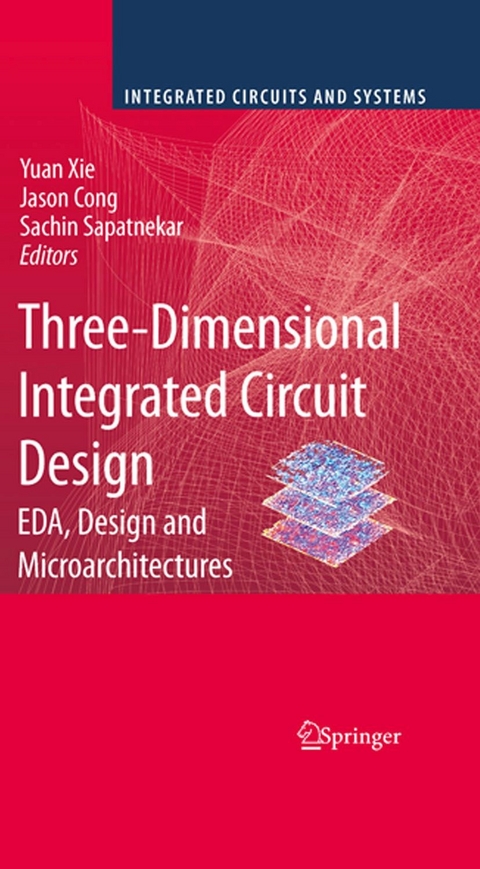
Three-Dimensional Integrated Circuit Design (eBook)
XII, 284 Seiten
Springer US (Verlag)
978-1-4419-0784-4 (ISBN)
We live in a time of great change. In the electronics world, the last several decades have seen unprecedented growth and advancement, described by Moore's law. This observation stated that transistor density in integrated circuits doubles every 1. 5-2 years. This came with the simultaneous improvement of individual device perf- mance as well as the reduction of device power such that the total power of the resulting ICs remained under control. No trend remains constant forever, and this is unfortunately the case with Moore's law. The trouble began a number of years ago when CMOS devices were no longer able to proceed along the classical scaling trends. Key device parameters such as gate oxide thickness were simply no longer able to scale. As a result, device o- state currents began to creep up at an alarming rate. These continuing problems with classical scaling have led to a leveling off of IC clock speeds to the range of several GHz. Of course, chips can be clocked higher but the thermal issues become unmanageable. This has led to the recent trend toward microprocessors with mul- ple cores, each running at a few GHz at the most. The goal is to continue improving performance via parallelism by adding more and more cores instead of increasing speed. The challenge here is to ensure that general purpose codes can be ef?ciently parallelized. There is another potential solution to the problem of how to improve CMOS technology performance: three-dimensional integrated circuits (3D ICs).
Foreword 5
Preface 7
Contents 9
Contributors 10
1 Introduction 12
References 24
2 3D Process Technology Considerations 25
2.1 Introduction 25
2.2 Background: Early Steps in the Emergence of 3D Integration 27
2.3 Process Factors That Impact State-of-the-Art 3D Design 28
2.3.1 Strata Orientation: Face-to-Back vs. Face-to-Face 28
2.3.1.1 Face-to-Back 28
2.3.1.2 Face-to-Face 29
2.3.2 Inter-strata Alignment: Tolerances for Inter-layer Connections 30
2.3.3 Bonding-Interface Design 32
2.3.3.1 Copper-to-Copper Compression Bonding 32
2.3.3.2 Hybrid Cu/Adhesive Bonding (Transfer-Join) 32
2.3.3.3 Oxide-Fusion Bonding 34
2.3.4 TSV Dimensions: Design Point Selection 35
2.3.4.1 Design Considerations for Tungsten and Copper TSVs 35
2.3.4.2 Ultra-High Density Vias Using SOI-Based 3D Integration 37
2.3.5 Via-Process Integration and a Reclassification of Via Types 38
2.3.5.1 Pre-backend Frontside Via (Type F1) 39
2.3.5.2 Post-backend Frontside Via (Type F2) 40
2.3.5.3 Backside Via (After Wafer Thinning, Type B) 40
2.4 Conclusion 40
References 41
3 Thermal and Power Delivery Challenges in 3D ICs 43
3.1 Introduction 43
3.2 Thermal Issues in 3D ICs 44
3.2.1 The Thermal PDE 44
3.2.2 Steady-State Thermal Analysis Algorithms 45
3.2.2.1 Formulation of the FDM Equations 46
3.2.3 The Finite Element Method 49
3.2.4 Thermal Optimization of 3D Circuits 52
3.3 Power Delivery in 3D ICs 53
3.3.1 The Basics of Power Delivery 53
3.3.2 Three-Dimensional IC Power Delivery: Modeling and Challenges 55
3.3.3 Design Techniques for Controlling PSN Noise 59
3.3.3.1 On-Chip Voltage Regulation 59
3.3.3.2 Z -axis Power Delivery 60
3.3.3.3 Multistory Power Delivery 61
3.3.4 CAD Techniques for Controlling PSN Noise 64
3.3.4.1 Decap Allocation 64
3.3.4.2 Automated MSPD Assignments for 3D ICs 66
3.4 Conclusion 68
References 68
4 Thermal-Aware 3D Floorplan 72
4.1 Introduction 72
4.2 Problem Formulation 73
4.2.1 3D Floorplanning with 2D Blocks 74
4.2.2 3D Floorplanning with 3D Blocks 75
4.3 Representations for 3D Floorplanning with 2D Blocks 76
4.3.1 Basic Representations for 2D Packing 76
4.3.1.1 Slicing Structure 77
4.3.1.2 Mosaic Structure 78
4.3.1.3 General Structure 79
4.3.1.4 Compact Structure 80
4.3.2 Analysis of Different Representations 82
4.3.2.1 Complexity 82
4.3.2.2 Redundancy 84
4.3.2.3 Suitability for 3D Design 86
4.4 Representations for the 3D Floorplan with 3D Blocks 86
4.4.1 3D Slicing Tree 87
4.4.2 3D Cbl 87
4.4.3 Sequence Triple 89
4.4.4 Analysis of Various Representations 91
4.5 Optimization Techniques 92
4.5.1 Simulated Annealing 93
4.5.2 SA-Based 3D Floorplanning with 2D Blocks 94
4.5.3 SA-Based 3D Floorplanning with 3D Blocks 95
4.5.4 Analytical Approach 97
4.6 Effects of Various 3D Floorplanning Techniques 100
4.6.1 Effects of 3D Floorplanning with 2D Blocks 100
4.6.2 Effects of 3D Floorplanning with 3D Blocks 102
4.7 Summary and Conclusion 104
4.8 Appendix: Design of Folded 3D Components 105
References 109
5 Thermal-Aware 3D Placement 112
5.1 Introduction 112
5.1.1 Problem Formulation 113
5.1.1.1 Wirelength Objective Function 113
5.1.1.2 Overlap-Free Constraints 114
5.1.1.3 Thermal Awareness 115
5.1.2 Overview of Existing 3D Placement Techniques 115
5.2 Partitioning-Based Techniques 116
5.3 Quadratic Uniformity Modeling Techniques 119
5.3.1 Wirelength Objective Function 121
5.3.2 Cell Distribution Cost Function 121
5.3.3 Thermal Distribution Cost Function 123
5.4 Multilevel Placement Technique 124
5.4.1 3D Placement Flow 124
5.4.2 Analytical Placement Engine 124
5.4.2.1 Relaxation of Discrete Variables 125
5.4.2.2 Log-Sum-Exp Wirelength 125
5.4.2.3 TS Via Number 126
5.4.2.4 Density Penalty Function 126
5.4.3 Multilevel Framework 130
5.5 Transformation-Based Techniques 130
5.5.1 Local Stacking Transformation Scheme 131
5.5.2 Folding Transformation Schemes 132
5.5.3 Window-Based Stacking/Folding Transformation Scheme 133
5.6 Legalization and Detailed Placement Techniques 134
5.6.1 Coarse Legalization 134
5.6.2 Detailed Legalization 136
5.6.2.1 DAG-Based Legalization 136
5.6.2.2 Tetris-Style Legalization 136
5.6.3 Layer Reassignment Through RCN Graph 138
5.6.3.1 Conflict-Net Graph 138
5.6.3.2 Relaxed Non-overlap Constraint 139
5.7 3D Placement Flow 139
5.8 Effects of Various 3D Placement Techniques 140
5.8.1 Trade-Offs Between Wirelength and TS Via Number 140
5.8.2 Effects of Thermal Optimization 145
5.8.2.1 Effects of the Thermal-Aware Net Weights on Temperature 145
5.8.2.2 Effects of the Legalization on Temperature 146
5.9 Impact of 3D Placement on Wirelength and Repeater Usage 146
5.9.1 2D/3D Placers and Repeater Estimation 147
5.9.2 Experimental Setup and Results 147
5.10 Summary and Conclusion 149
References 151
6 Thermal Via Insertion and Thermally Aware Routing in 3D ICs 154
6.1 Introduction 154
6.2 Thermal Vias 155
6.3 Inserting Thermal Vias into a Placed Design 156
6.4 Routing Algorithms 161
6.4.1 A Multilevel Approach 162
6.4.2 A Two-Phase Approach Using Linear Programming 164
6.5 Conclusion 168
References 168
7 Three-Dimensional Microprocessor Design 170
7.1 Introduction 170
7.2 Stacking Complete Modules 171
7.2.1 Three-Dimensional Stacked Caches 172
7.2.2 Optional Functionality 175
7.2.2.1 Introspective 3D Processors 175
7.2.2.2 Reliable 3D Processors 177
7.2.2.3 TSV Requirements 179
7.2.3 System-Level Integration 179
7.3 Stacking Functional Unit Blocks 179
7.3.1 Removing Wires 180
7.3.2 TSV Requirements 182
7.3.3 Design Space Issues 184
7.4 Splitting Functional Unit Blocks 184
7.4.1 Tradeoffs in 3D Cache Organizations 184
7.4.1.1 Three Dimension Splitting the Cache 186
7.4.1.2 Dealing with TSVs 189
7.4.2 Three Dimensional-Splitting Arithmetic Units 191
7.4.3 Three-Dimensional Adders 191
7.4.4 Interfacing Units 192
7.5 Conclusions 194
References 196
8 Three-Dimensional Network-on-Chip Architecture 198
8.1 Introduction 198
8.2 A Brief Introduction on Network-on-Chip 200
8.2.1 NoC Topology 201
8.2.2 NoC Router Design 202
8.2.3 More Information on NoC Design 203
8.3 Three-Dimensional NoC Architectures 203
8.3.1 Symmetric NoC Router Design 204
8.3.2 Three-Dimensional NoC--Bus Hybrid Router Design 206
8.3.3 True 3D Router Design 207
8.3.4 3D Dimensionally-Decomposed NoC Router Design 210
8.3.5 Multi-layer 3D NoC Router Design 210
8.3.6 3D NoC Topology Design 212
8.3.7 Impact of 3D Technology on NoC Designs 212
8.4 Chip Multiprocessor Design with 3D NoC Architecture 213
8.4.1 The 3D L2 Cache Stacking on CMP Architecture 214
8.4.2 The dTDMA Bus as a Communication Pillar 215
8.4.3 3D NoC--Bus Hybrid Router Architecture 217
8.4.4 Processors and L2 Cache Organization 218
8.4.5 Cache Management Policies 218
8.4.5.1 Search Policy 218
8.4.5.2 Placement and Replacement Policy 219
8.4.5.3 Cache Line Migration Policy 220
8.4.6 Methodology 220
8.4.7 Results 221
8.5 Conclusion 224
References 225
9 PicoServer: Using 3D Stacking Technology to Build Energy Efficient Servers 227
9.1 Introduction 227
9.2 Background 230
9.2.1 Server Platforms 231
9.2.1.1 Three-Tier Server Architecture 231
9.2.1.2 Server Workload Characteristics 232
9.2.1.3 Conventional Server Power Breakdown 233
9.2.2 Three-Dimensional Stacking Technology 234
9.2.3 DRAM Technology 235
9.3 Methodology 236
9.3.1 Simulation Studies 236
9.3.1.1 Full System Architectural Simulator 236
9.3.1.2 Server Benchmarks 237
9.3.2 Estimating Power and Area 239
9.3.2.1 Processors 239
9.3.2.2 Interconnect Considering 3D Stacking Technology 240
9.3.2.3 DRAM 241
9.3.2.4 Network Interface Controller -- NIC 242
9.4 PicoServer Architecture 242
9.4.1 Core Architecture and the Impact of Multithreading 243
9.4.2 Wide Shared Bus Architecture 245
9.4.3 On-chip DRAM Architecture 246
9.4.3.1 Role of On-chip DRAM 246
9.4.3.2 On-Chip DRAM Interface 248
9.4.3.3 Impact of On-Chip DRAM Refresh on Throughput 249
9.4.4 The Need for Multiple NICs on a CMP Architecture 249
9.4.5 Thermal Concerns in 3D Stacking 250
9.4.6 Impact of Integrating Flash onto PicoServer 252
9.5 Results 257
9.5.1 Overall Performance 258
9.5.2 Overall Power 261
9.5.3 Energy Efficiency Pareto Chart 262
9.6 Conclusions 263
References 265
10 System-Level 3D IC Cost Analysis and Design Exploration 269
10.1 Introduction 269
10.2 Early Design Estimation for 3D ICs 270
10.2.1 The Preliminary on Rent's Rule 271
10.2.2 Die Area and Metal Layer Estimator 272
10.2.3 The Impact of TSVs 273
10.3 Three-Dimensional Cost Model 274
10.4 System-Level 3D IC Design Exploration 277
10.4.1 Evaluation of the TSV's Impact on Die Area 278
10.4.2 The Potential of Metal Layer Reduction in 3D ICs 278
10.4.3 Bonding Techniques: D2W or W2W 279
10.4.4 Cost vs. Number of 3D Layers 280
10.4.5 Heterogenous Stacking 281
10.5 Cost-Driven 3D Design Flow 282
10.5.1 Case Study: Two-Layer OpenSPARC T1 3D Processor 285
10.6 Reciprocal Design Symmetry for Mask Reuse in 3D ICs 285
10.7 Conclusion 287
References 287
Index 289
| Erscheint lt. Verlag | 2.12.2009 |
|---|---|
| Reihe/Serie | Integrated Circuits and Systems |
| Zusatzinfo | XII, 284 p. |
| Verlagsort | New York |
| Sprache | englisch |
| Themenwelt | Naturwissenschaften ► Chemie ► Technische Chemie |
| Technik ► Elektrotechnik / Energietechnik | |
| Technik ► Maschinenbau | |
| Schlagworte | Automation • Circuit Design • Design • FPGA • Integrated circuit • microprocessor • Network • Technology |
| ISBN-10 | 1-4419-0784-X / 144190784X |
| ISBN-13 | 978-1-4419-0784-4 / 9781441907844 |
| Haben Sie eine Frage zum Produkt? |
Größe: 8,9 MB
DRM: Digitales Wasserzeichen
Dieses eBook enthält ein digitales Wasserzeichen und ist damit für Sie personalisiert. Bei einer missbräuchlichen Weitergabe des eBooks an Dritte ist eine Rückverfolgung an die Quelle möglich.
Dateiformat: PDF (Portable Document Format)
Mit einem festen Seitenlayout eignet sich die PDF besonders für Fachbücher mit Spalten, Tabellen und Abbildungen. Eine PDF kann auf fast allen Geräten angezeigt werden, ist aber für kleine Displays (Smartphone, eReader) nur eingeschränkt geeignet.
Systemvoraussetzungen:
PC/Mac: Mit einem PC oder Mac können Sie dieses eBook lesen. Sie benötigen dafür einen PDF-Viewer - z.B. den Adobe Reader oder Adobe Digital Editions.
eReader: Dieses eBook kann mit (fast) allen eBook-Readern gelesen werden. Mit dem amazon-Kindle ist es aber nicht kompatibel.
Smartphone/Tablet: Egal ob Apple oder Android, dieses eBook können Sie lesen. Sie benötigen dafür einen PDF-Viewer - z.B. die kostenlose Adobe Digital Editions-App.
Zusätzliches Feature: Online Lesen
Dieses eBook können Sie zusätzlich zum Download auch online im Webbrowser lesen.
Buying eBooks from abroad
For tax law reasons we can sell eBooks just within Germany and Switzerland. Regrettably we cannot fulfill eBook-orders from other countries.
aus dem Bereich


