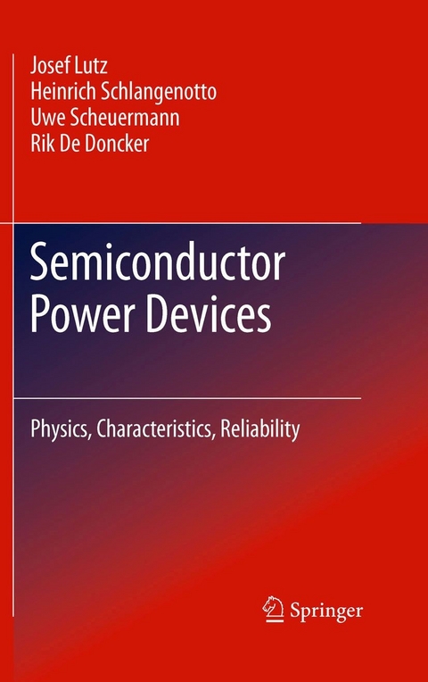
Semiconductor Power Devices (eBook)
XII, 536 Seiten
Springer Berlin (Verlag)
978-3-642-11125-9 (ISBN)
Josef Lutz joined Semikron in Nuremberg, Germany, in 1983. First he worked in the development of GTO thyristors, then in the field of fast recovery diodes. He introduced the Controlled Axial Lifetime (CAL) diode, is holder of several patents regarding fast diodes, and has published more than 100 papers and conference contributions. In 1999 he received his Ph.D. in electrical engineering at the University of Ilmenau, Germany. Since August 2001 he is Professor for Power Electronics and Electromagnetic Compatibility at the Chemnitz University of Technology, Germany. He is member of the board of directors of the ZfM, of the International Steering Committee of the EPE, advisory board of the PCIM, of the program committee of the ISPS and CIPS. In 2005 he was awarded the rank of an honourable professor at the North Caucasus State Technical University in Stavropol. Uwe Scheuermann joined Semikron in Nuremberg, Germany, after completing his Ph.D. in semiconductor physics in 1990. After spending 5 years with the development of diode and thyristor chips, he changed his focus to the development of power modules. He has been involved in the development of the advanced power module families without base plates and the implementation of new packaging concepts like spring contacts. He has published more than 30 papers and holds several patents in the field of packaging technology. Today, he is at Semikron responsible for the reliability of components. He is a member of the board of directors of the PCIM Europe and of the program committee of the CIPS. Since 2006 he is engaged as an external lecturer at the Friedrich-Alexander-University of Erlangen. Rik De Doncker received his degree of Doctor in Electrical Engineering from the Katholieke Universiteit Leuven, Belgium in 1986. During 1987 he was appointed Visiting Associate Professor at the University of Wisconsin, Madison. In 1988, he was employed as a General Electric Company fellow at the microelectronic center IMEC, Leuven, Belgium. In Dec. 1988, he joined the General Electric Company at the Corporate Research and Development Center, Schenectady, NY where he led research on drives and high power soft-switching converters, ranging from 100 kW to 4 MW, for aerospace, industrial and traction applications. In 1994 he joined Silicon Power Corporation (formerly GE-SPCO) as Vice President Technology where he worked on high power converter systems and MTO devices and was responsible for the development and production of world's first 15 kV medium voltage transfer switch. Since Oct. 1996 he became professor at the RWTH-Aachen, where he leads the Institute für Stromrichtertechnik und Elektrische Antriebe (ISEA). In Oct. 2006 he became director of the E.ON Energy Research Center at RWTH Aachen University. Heinrich Schlangenotto received the Ph.D. degree in theoretical physics at the University of Münster, in 1966 he joined the Research Institute of AEG-Telefunken in Frankfurt. Working on operation principles of semiconductor power devices, he improved the description of forward conduction based on a new insight in the spatial distribution of recombination. Investigating the injection and temperature dependence of radiative recombination, which is used in analyzing device operation, he finds an important influence of exciton formation even near room temperature. A major point of his work was the development of device concepts such as the fast, soft recovery SPEED-diode. He gave the first quantitative description of the dynamical avalanche mechanism limiting fast switching. From 1991 to 2001 he held a lecture on power devices at the Technical University of Darmstadt. His results were published in many papers and conference reports.
Josef Lutz joined Semikron in Nuremberg, Germany, in 1983. First he worked in the development of GTO thyristors, then in the field of fast recovery diodes. He introduced the Controlled Axial Lifetime (CAL) diode, is holder of several patents regarding fast diodes, and has published more than 100 papers and conference contributions. In 1999 he received his Ph.D. in electrical engineering at the University of Ilmenau, Germany. Since August 2001 he is Professor for Power Electronics and Electromagnetic Compatibility at the Chemnitz University of Technology, Germany. He is member of the board of directors of the ZfM, of the International Steering Committee of the EPE, advisory board of the PCIM, of the program committee of the ISPS and CIPS. In 2005 he was awarded the rank of an honourable professor at the North Caucasus State Technical University in Stavropol. Uwe Scheuermann joined Semikron in Nuremberg, Germany, after completing his Ph.D. in semiconductor physics in 1990. After spending 5 years with the development of diode and thyristor chips, he changed his focus to the development of power modules. He has been involved in the development of the advanced power module families without base plates and the implementation of new packaging concepts like spring contacts. He has published more than 30 papers and holds several patents in the field of packaging technology. Today, he is at Semikron responsible for the reliability of components. He is a member of the board of directors of the PCIM Europe and of the program committee of the CIPS. Since 2006 he is engaged as an external lecturer at the Friedrich-Alexander-University of Erlangen. Rik De Doncker received his degree of Doctor in Electrical Engineering from the Katholieke Universiteit Leuven, Belgium in 1986. During 1987 he was appointed Visiting Associate Professor at the University of Wisconsin, Madison. In 1988, he was employed as a General Electric Company fellow at the microelectronic center IMEC, Leuven, Belgium. In Dec. 1988, he joined the General Electric Company at the Corporate Research and Development Center, Schenectady, NY where he led research on drives and high power soft-switching converters, ranging from 100 kW to 4 MW, for aerospace, industrial and traction applications. In 1994 he joined Silicon Power Corporation (formerly GE-SPCO) as Vice President Technology where he worked on high power converter systems and MTO devices and was responsible for the development and production of world’s first 15 kV medium voltage transfer switch. Since Oct. 1996 he became professor at the RWTH-Aachen, where he leads the Institute für Stromrichtertechnik und Elektrische Antriebe (ISEA). In Oct. 2006 he became director of the E.ON Energy Research Center at RWTH Aachen University. Heinrich Schlangenotto received the Ph.D. degree in theoretical physics at the University of Münster, in 1966 he joined the Research Institute of AEG-Telefunken in Frankfurt. Working on operation principles of semiconductor power devices, he improved the description of forward conduction based on a new insight in the spatial distribution of recombination. Investigating the injection and temperature dependence of radiative recombination, which is used in analyzing device operation, he finds an important influence of exciton formation even near room temperature. A major point of his work was the development of device concepts such as the fast, soft recovery SPEED-diode. He gave the first quantitative description of the dynamical avalanche mechanism limiting fast switching. From 1991 to 2001 he held a lecture on power devices at the Technical University of Darmstadt. His results were published in many papers and conference reports.
Semiconductor Power Devices 1
Preface 4
Contents 6
Chapter 1 Power Semiconductor Devices Key Components for Efficient Electrical Energy Conversion Systems 12
1.1 Systems, Power Converters, and Power Semiconductor Devices 12
1.1.1 Basic Principles of Power Converters 14
1.1.2 Types of Power Converters and Selection of Power Devices 15
1.2 Operating and Selecting Power Semiconductors 18
1.3 Applications of Power Semiconductors 21
References 25
Chapter 2 Semiconductor Properties 27
2.1 Introduction 27
2.2 Crystal Structure 29
2.3 Energy Gap and Intrinsic Concentration 31
2.4 Energy Band Structure and Particle Properties of Carriers 36
2.5 The Doped Semiconductor 40
2.6 Current Transport 49
2.6.1 Carrier Mobilities and Field Currents 49
2.6.2 High-Field Drift Velocities 55
2.6.3 Diffusion of Carriers and Current Transport Equations 56
2.7 Recombination-Generation and Lifetime of Non-equilibrium Carriers 58
2.7.1 Intrinsic Recombination Mechanisms 60
2.7.2 Recombination and Generation at Recombination Centers 61
2.8 Impact Ionization 70
2.9 Basic Equations of Semiconductor Devices 76
2.10 Simple Conclusions 79
References 82
Chapter 3 pn-Junctions 86
3.1 The pn-Junction in Thermal Equilibrium 86
3.1.1 The Abrupt Step Junction 89
3.1.2 Graded Junctions 95
3.2 CurrentVoltage Characteristics of the pn-Junction 98
3.3 Blocking Characteristics and Breakdown of the pn-Junction 107
3.3.1 Blocking Current 107
3.3.2 Avalanche Multiplication and Breakdown Voltage 110
Temperature Dependence 118
3.3.3 Blocking Capability with Wide-Gap Semiconductors 119
3.4 Injection Efficiency of Emitter Regions 120
3.5 Capacitance of pn-Junctions 127
References 129
Chapter 4 Short Introduction to Power Device Technology 131
4.1 Crystal Growth 131
4.2 Neutron Transmutation for Adjustment of the Wafer Doping 134
4.3 Epitaxial Growth 136
4.4 Diffusion 137
4.5 Ion Implantation 142
4.6 Oxidation and Masking 147
4.7 Edge Terminations 150
4.7.1 Bevelled Termination Structures 150
4.7.2 Planar Junction Termination Structures 152
4.7.3 Junction Termination for Bidirectional Blocking Devices 154
4.8 Passivation 155
4.9 Recombination Centers 156
4.9.1 Gold and Platinum as Recombination Centers 156
4.9.2 Radiation-Induced Recombination Centers 159
4.9.3 Radiation-Enhanced Diffusion of Pt and Pd 162
References 163
Chapter 5 pin-Diodes 166
5.1 Structure of the pin-Diode 166
5.2 I-V Characteristic of the pin-Diode 167
5.3 Design and Blocking Voltage of the pin-Diode 169
5.4 Forward Conduction Behavior 174
5.4.1 Carrier Distribution 174
5.4.2 Junction Voltages 177
5.4.3 Voltage Drop Across the Middle Region 179
5.4.4 Voltage Drop in the Hall Approximation 180
5.4.5 Emitter Recombination, Effective Carrier Lifetime, and Forward Characteristic 182
5.4.6 Temperature Dependency of the Forward Characteristics 190
5.5 Relation Between Stored Charge and Forward Voltage 191
5.6 Turn-On Behavior of Power Diodes 192
5.7 Reverse Recovery of Power Diodes 195
5.7.1 Definitions 195
5.7.2 Reverse Recovery Related Power Losses 201
5.7.3 Reverse Recovery: Charge Dynamic in the Diode 205
5.7.4 Fast Diodes with Optimized Reverse Recovery Behavior 213
5.7.4.1 Diodes with a Doping Step in the Low-Doped Layer 213
5.7.4.2 Diodes with Anode Structures for Improving the Recovery Behavior 214
5.7.4.3 The EMCON Diode 216
5.7.4.4 The CAL Diode CAL-diode 218
5.7.4.5 The Hybrid Diode 220
5.7.4.6 The Tandem Diode 222
5.7.4.7 MOS-Controlled Diodes 223
5.7.4.8 Diodes with Cathode Side Hole Injection 228
5.8 Outlook 229
References 230
Chapter 6 Schottky Diodes 232
6.1 Aspects of the Physics of the MetalSemiconductor Junction 232
6.2 CurrentVoltage Characteristics of the Schottky Junction 234
6.3 Structure of Schottky Diodes 237
6.4 Ohmic Voltage Drop of a Unipolar Device 237
Example: Design of a Silicon Schottky Diode for a Rated Voltage of 200 V 240
6.5 Schottky Diodes Based on SiC 241
References 246
Chapter 7 Bipolar Transistors 248
7.1 Function of the Bipolar Transistor 248
7.2 Structure of the Bipolar Power Transistor 250
7.3 I-V Characteristic of the Power Transistor 251
7.4 Blocking Behavior of the Bipolar Power Transistor 252
7.5 Current Gain of the Bipolar Transistor 254
7.6 Base Widening, Field Redistribution, and Second Breakdown 258
7.7 Limits of the Silicon Bipolar Transistor 261
7.8 SiC Bipolar Transistor 262
References 263
Chapter 8 Thyristors 264
8.1 Structure and Mode of Function 264
8.2 I-V Characteristic of the Thyristor 267
8.3 Blocking Behavior of the Thyristor 269
8.4 The Function of Emitter Shorts 271
8.5 Modes to Trigger a Thyristor 272
8.6 Trigger Front Spreading 273
8.7 Follow-Up Triggering and Amplifying Gate 274
8.8 Thyristor Turn-Off and Recovery Time 277
8.9 The Triac 279
8.10 The Gate Turn-Off Thyristor (GTO) 280
8.11 The Gate-Commutated Thyristor (GCT) 286
References 288
Chapter 9 MOS Transistors 290
9.1 Function Principle of the MOSFET 290
9.2 Structure of Power MOSFETs 292
9.3 CurrentVoltage Characteristics of MOS Transistors 294
9.4 Characteristics of the MOSFET Channel 295
9.5 The Ohmic Region 299
9.6 Compensation Structures in Modern MOSFETs 300
9.7 Switching Properties of the MOSFET 305
9.8 Switching Losses of the MOSFET 309
9.9 Safe Operating Area of the MOSFET 310
9.10 The Inverse Diode of the MOSFET 312
9.11 SiC Field Effect Devices 316
9.12 Outlook 319
References 319
Chapter 10 IGBTs 322
10.1 Mode of Function 322
10.2 The IV Characteristic of the IGBT 324
10.3 The Switching Behavior of the IGBT 326
10.4 The Basic Types: PT-IGBT and NPT-IGBT 328
10.5 Plasma Distribution in the IGBT 332
10.6 Modern IGBTs with Increased Charge Carrier Density 334
10.6.1 Plasma Enhancement by High n-Emitter Efficiency 334
10.6.2 The ''Latch-Up Free Cell Geometry'' 338
10.6.3 The Effect of the ''Hole Barrier'' 339
10.6.4 Collector Side Buffer Layers 341
10.7 IGBTs with Bidirectional Blocking Capability 342
10.8 Reverse Conducting IGBT reverse conducting IGBT s 344
10.9 Outlook 347
References 347
Chapter 11 Packaging and Reliability of Power Devices 350
11.1 The Challenge of Packaging Technology 350
11.2 Package Types 351
11.2.1 Capsules 353
11.2.2 The TO Family and Its Relatives 355
11.2.3 Modules 360
11.3 Physical Properties of Materials 365
11.4 Thermal Simulation and Thermal Equivalent Circuits 367
11.4.1 Transformation Between Thermo-dynamicaland Electrical Parameters 367
11.4.2 One-Dimensional Equivalent Networks 374
11.4.3 The Three-Dimensional Thermal Network 376
11.4.4 The Transient Thermal Resistance 377
11.5 Parasitic Electrical Elements in Power Modules 380
11.5.1 Parasitic Resistances 380
11.5.2 Parasitic Inductance 381
11.5.3 Parasitic Capacities 385
11.6 Reliability 387
11.6.1 The Demand for Increasing Reliability 387
11.6.2 High Temperature Reverse Bias Test 390
11.6.3 High Temperature Gate Stress Test 392
11.6.4 Temperature Humidity Bias Test 393
11.6.5 High Temperature and Low Temperature Storage Tests 394
11.6.6 Temperature Cycling and Temperature Shock Test 395
11.6.7 Power Cycling Test 397
11.6.7.1 Weibull Statistics for Power Cycling Analysis 400
11.6.7.2 Models for Lifetime Prediction 401
11.6.7.3 Superimposition of Power Cycles 404
11.6.7.4 Bond Wire Lift-Off 406
11.6.7.5 Reconstruction of Metallization 407
11.6.7.6 Solder Fatigue 410
11.6.7.7 Power Cycling Capability of Molded TO Package 414
11.6.7.8 Comparability of Power Cycling Lifetime Curves 416
11.6.8 Additional Reliability Tests 417
11.6.9 Strategies for Enhanced Reliability 418
11.7 Future Challenges 419
References 423
Chapter 12 Destructive Mechanisms in Power Devices 426
12.1 Thermal Breakdown Failures by Excess Temperature 426
12.2 Surge Current 428
12.3 Overvoltage Voltage Above Blocking Capability 433
12.4 Dynamic Avalanche 439
12.4.1 Dynamic Avalanche in Bipolar Devices 439
12.4.2 Dynamic Avalanche in Fast Diodes 440
Dynamic Avalanche of the First Degree 440
Dynamic Avalanche of the Second Degree 442
Dynamic Avalanche of the Third Degree 444
12.4.3 Diode Structures with High Dynamic Avalanche Capability 449
12.4.4 Dynamic Avalanche: Further Tasks 453
12.5 Exceeding the Maximum Turn-Off Current of GTOs 453
12.6 Short-Circuit and Over-Current in IGBTs 454
12.6.1 Short-Circuit Types I, II, and III 454
12.6.2 Thermal and Electrical Stress in Short Circuit 459
Thermal Limits for Medium-Voltage IGBTs 462
Current Filamentation as Limit for the Short-Circuit Capability of High-Voltage IGBTs 465
12.6.3 Turn-Off of Over-Current and Dynamic Avalanche 467
12.7 Cosmic Ray Failures 469
12.8 Failure Analysis 475
References 477
Chapter 13 Power Device-Induced Oscillations and Electromagnetic Disturbances 481
13.1 Frequency Range of Electromagnetic Disturbances 481
Harmonics 482
13.2 LC Oscillations 483
13.2.1 Turn-Off Oscillations with IGBTs Connected in Parallel 483
13.2.2 Turn-Off Oscillations with Snappy Diodes 486
13.3 Transit-Time Oscillations 489
13.3.1 Plasma-Extraction Transit-Time (PETT) Oscillations 489
13.3.2 Dynamic Impact-Ionization Transit-Time (IMPATT) Oscillations 497
References 501
Chapter 14 Power Electronic Systems 502
14.1 Definition and Basic Features 502
14.2 Monolithically Integrated Systems Power ICs 504
14.3 System Integration on Printed Circuit Board 508
14.4 Hybrid Integration 510
References 517
Appendix A Modeling Parameters of Carrier Mobilities in Si and 4H-SiC 519
A.1 Mobilities in Silicon 519
A.2 Mobilities in 4H-SiC 520
Appendix B: Avalanche Multiplication Factors and Effective Ionization Rate 521
B.1 Multiplication Factors 521
B.2 Effective Ionization Rate and Breakdown Condition 523
References for Appendices A and B 523
Appendix C Thermal Parameters of Important Materials in Packaging Technology 525
Appendix D Electric Parameters of Important Materials 526
References for Appendices C and D 527
Appendix E: Often Used Symbols 528
Remark 530
Index 531
| Erscheint lt. Verlag | 15.1.2011 |
|---|---|
| Zusatzinfo | XII, 536 p. |
| Verlagsort | Berlin |
| Sprache | englisch |
| Original-Titel | Halbleiter-Leistungsbauelemente |
| Themenwelt | Naturwissenschaften ► Physik / Astronomie |
| Technik ► Elektrotechnik / Energietechnik | |
| Technik ► Maschinenbau | |
| Schlagworte | Fast Diodes • IGBT • MOFSET • Packaging Technology |
| ISBN-10 | 3-642-11125-4 / 3642111254 |
| ISBN-13 | 978-3-642-11125-9 / 9783642111259 |
| Haben Sie eine Frage zum Produkt? |
Größe: 20,2 MB
DRM: Digitales Wasserzeichen
Dieses eBook enthält ein digitales Wasserzeichen und ist damit für Sie personalisiert. Bei einer missbräuchlichen Weitergabe des eBooks an Dritte ist eine Rückverfolgung an die Quelle möglich.
Dateiformat: PDF (Portable Document Format)
Mit einem festen Seitenlayout eignet sich die PDF besonders für Fachbücher mit Spalten, Tabellen und Abbildungen. Eine PDF kann auf fast allen Geräten angezeigt werden, ist aber für kleine Displays (Smartphone, eReader) nur eingeschränkt geeignet.
Systemvoraussetzungen:
PC/Mac: Mit einem PC oder Mac können Sie dieses eBook lesen. Sie benötigen dafür einen PDF-Viewer - z.B. den Adobe Reader oder Adobe Digital Editions.
eReader: Dieses eBook kann mit (fast) allen eBook-Readern gelesen werden. Mit dem amazon-Kindle ist es aber nicht kompatibel.
Smartphone/Tablet: Egal ob Apple oder Android, dieses eBook können Sie lesen. Sie benötigen dafür einen PDF-Viewer - z.B. die kostenlose Adobe Digital Editions-App.
Buying eBooks from abroad
For tax law reasons we can sell eBooks just within Germany and Switzerland. Regrettably we cannot fulfill eBook-orders from other countries.
aus dem Bereich


