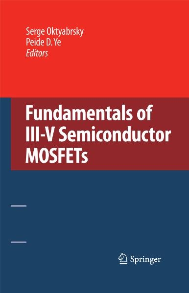
Fundamentals of III-V Semiconductor MOSFETs (eBook)
XV, 445 Seiten
Springer US (Verlag)
978-1-4419-1547-4 (ISBN)
Fundamentals of III-V Semiconductor MOSFETs presents the fundamentals and current status of research of compound semiconductor metal-oxide-semiconductor field-effect transistors (MOSFETs) that are envisioned as a future replacement of silicon in digital circuits. The material covered begins with a review of specific properties of III-V semiconductors and available technologies making them attractive to MOSFET technology, such as band-engineered heterostructures, effect of strain, nanoscale control during epitaxial growth. Due to the lack of thermodynamically stable native oxides on III-V's (such as SiO2 on Si), high-k oxides are the natural choice of dielectrics for III-V MOSFETs. The key challenge of the III-V MOSFET technology is a high-quality, thermodynamically stable gate dielectric that passivates the interface states, similar to SiO2 on Si. Several chapters give a detailed description of materials science and electronic behavior of various dielectrics and related interfaces, as well as physics of fabricated devices and MOSFET fabrication technologies. Topics also include recent progress and understanding of various materials systems; specific issues for electrical measurement of gate stacks and FETs with low and wide bandgap channels and high interface trap density; possible paths of integration of different semiconductor materials on Si platform.
Fundamentals of III-V Semiconductor MOSFETs presents the fundamentals and current status of research of compound semiconductor metal-oxide-semiconductor field-effect transistors (MOSFETs) that are envisioned as a future replacement of silicon in digital circuits. The material covered begins with a review of specific properties of III-V semiconductors and available technologies making them attractive to MOSFET technology, such as band-engineered heterostructures, effect of strain, nanoscale control during epitaxial growth. Due to the lack of thermodynamically stable native oxides on III-V's (such as SiO2 on Si), high-k oxides are the natural choice of dielectrics for III-V MOSFETs. The key challenge of the III-V MOSFET technology is a high-quality, thermodynamically stable gate dielectric that passivates the interface states, similar to SiO2 on Si. Several chapters give a detailed description of materials science and electronic behavior of various dielectrics and related interfaces, as well as physics of fabricated devices and MOSFET fabrication technologies. Topics also include recent progress and understanding of various materials systems; specific issues for electrical measurement of gate stacks and FETs with low and wide bandgap channels and high interface trap density; possible paths of integration of different semiconductor materials on Si platform.
Preface 5
Contents 8
Contributors 12
Non-Silicon MOSFET Technology: A Long Time Coming 15
Abstract 15
1.1 Introduction 15
1.2 Brief and Non-Comprehensive History of the NSMOSFET 16
1.3 Surface Fermi Level Pinning: The Bane of NSMOSFET Technology Development 17
1.4 Concluding Remarks 20
References 20
Properties and Trade-Offs of Compound Semiconductor MOSFETs 21
2.1 Introduction 21
2.2 Simulation Framework 24
2.2.1 Bandstructure Calculation (Real and Complex) 24
2.2.2 Band-to-Band Tunneling (Off-State Leakage) 25
2.2.3 Quantum Ballistic Current (On-State Drive Current) 27
2.3 Power-Performance Tradeoffs in Binary III-V Materials (GaAs, InAs, InP and InSb) vs. Si and Ge 29
2.3.1 Inversion Charge and Injection Velocity 29
2.3.2 ION., IOFF, BTBT and Delay 30
2.3.3 Effect of Scaling Film Thickness and VDD 31
2.3.4 Power-Performance Tradeoff of Binary III-V Materials vs. Si and Ge 32
2.4 Power-Performance of Strained Ternary III-V Material (InxGa1-xAs) 33
2.4.1 Strained InGaAs Band Structures 33
2.4.2 ION and IOFF,BTBT with Strain Engineering and Channel Orientation 34
2.4.3 Power-Performance of Strained Ternary III-V Material (InGaAs) 35
2.5 Strained III-V for p-MOSFETs 36
2.5.1 Hole Mobility in Ternary III-V Materials (InGaAs vs. InGaSb) 36
2.5.2 Hole Mobility Enhancement in III-Vs with Strain 37
2.6 Novel Device Structure and Parasitics 38
2.6.1 Quantum Well (QW) Strained Heterostructure III-V FETs 38
2.6.2 Parasitic Resistance 39
2.6.3 Parasitic Capacitance 40
2.7 Conclusion 41
Device Physics and Performance Potential of III-V Field-Effect Transistors 45
3.1 Introduction 45
3.2 InGaAs HEMTs 46
3.2.1 Device Structure 46
3.2.2 Simulation Approach 48
3.2.3 Materials Parameters 48
3.2.4 Results 49
3.3 Discussion 50
3.3.1 Gate Capacitance 50
3.3.2 Charge Control in a Nanoscale HEMT 52
3.3.3 Velocity at the Virtual Source 53
3.3.4 Ballistic Mobility 54
3.3.5 Source Design Issues 55
3.3.6 Role of S/D Tunneling 56
3.3.7 Back of the Envelope Calculations 58
3.4 Conclusions 60
Theory of HfO2-Based High-k Dielectric Gate Stacks 64
4.1 Introduction 64
4.2 Theoretical Background 65
4.2.1 Density Functional Theory 65
4.2.2 Modeling Interfaces and Surfaces 68
4.3 Properties of Bulk Hafnia and Zirconia 70
4.4 Surfaces 84
4.4.1 Monoclinic Hafnia 85
4.4.2 Tetragonal Hafnia 91
4.4.3 Role of Surface Energy in the M–T Transformation 93
4.5 Band Alignment at Hafnia Interfaces 94
4.5.1 SiO2.../.HfO2 Interface 95
4.5.2 Effects of Al Doping at the SiO2./HfO2 Interface 97
4.5.3 Thermal Stability and Fermi Level Pinning at the HfO2./Metal Interface 99
4.6 Conclusions 102
Density Functional Theory Simulations of High-k Oxides on III-V Semiconductors 105
5.1 Introduction 105
5.1.1 High-k Oxides 105
5.1.2 III-V Semiconductors 106
5.1.3 Density-Functional Theory 107
5.2 Methodology of DFT Simulations of High-k Oxides on Semiconductor Substrates 108
5.2.1 Oxide Deposition Technique in DFT Simulations 108
5.2.2 Oxide-Semiconductor Stack Design 110
5.2.3 Crystalline vs. Amorphous Oxides in DFT Simulations 113
5.2.4 The Oxide-Semiconductor Stack Simulation Techniques: DFT Relaxation vs. Molecular Dynamics 115
5.3 DFT Simulations of High-k Oxides on Si/Ge Substrates 118
5.4 Generation of Amorphous High-k Oxide Samples by Hybrid Classical-DFT Molecular Dynamics Computer Simulations 124
5.5 The Current Progress in DFT Simulations of High-k Oxide/III-V Semiconductor Stacks 130
5.5.1 Interfacial Bonding Structure 132
5.5.2 Density of State Analysis 133
5.5.3 Semiconductor Substrate Deformation 134
5.5.4 Bader Charge Analysis 135
5.5.5 Comparison to Experimental Data 136
5.5.5.1 a-Al2O3/InAlAs 136
5.5.5.2 a-Al2O3/InGaAs 137
5.6 Summary 138
Interfacial Chemistry of Oxides on III-V Compound Semiconductors 143
6.1 Introduction 143
6.2 Surfaces of III-V MOSFET Semiconductor Candidates 144
6.2.1 GaAs 145
6.2.2 GaAs/InAs Alloys: InGaAs 148
6.2.3 Phosphides and Antimonides 149
6.3 Oxide Formation (Native and Thermal) 150
6.3.1 Stable Oxidation States on InxGa(1-x)As 150
6.3.2 Ga-Suboxides 154
6.3.3 Oxides of Antimonides 157
6.3.4 Oxides of Phosphides 158
6.4 Oxide Deposition on III-V Substrates 158
6.4.1 Preparation of III-V Substrate Surfaces 159
6.4.2 Atomic Layer Deposition (ALD) on III-V Substrate Surfaces 160
6.4.2.1 ALD on GaAs 161
6.4.2.2 ALD on InGaAs 165
6.4.2 Atomic Layer Deposition (ALD) on III-VSubstrate Surfaces 160
6.4.2.1 ALD on GaAs 161
6.4.2.2 ALD on InGaAs 165
6.5 Electrical Behavior of Oxides on III-V and Interfacial Chemistry 168
6.5.1 C–V Measurements and Issues 168
6.5.1.1 Frequency Dispersion 168
6.5.1.2 Hasegawa and Sawada Cit Model 171
6.5.1.3 Detection of Free Carriers 172
6.5.2 Interface States of InxGa1-xAs 173
6.5.2.1 Effect of Silicon Interfacial Passivation Layer (IPL) 173
6.5.3 Effect of Indium Concentration 175
6.6 Conclusions 177
Atomic-Layer Deposited High-k/III-V Metal-Oxide-Semiconductor Devices and Correlated Empirical Model 185
7.1 Introduction 185
7.2 History and Current Status 186
7.3 Empirical Model for III-V MOS Interfaces 190
7.4 Experiments on High-k/III-V MOSFETs 193
7.4.1 High-k/GaAs MOSFETs 193
7.4.2 High-k/InxGa1-xAs MOSFETs 195
7.4.3 High-k/InP MOSFETs 197
7.4.4 High-k/GaSb MOSFETs 198
7.5 Conclusion 200
Materials and Technologies for III-V MOSFETs 206
8.1 Introduction 206
8.2 III-V HEMTs for Digital Applications 207
8.2.1 Intrinsic Delay 210
8.2.2 Dynamic Power 213
8.2.3 Static Power 215
8.2.4 Enhancement Mode HEMTs 217
8.2.5 Recessed Gate Technology 217
8.3 Challenges for III-V MOSFETs 218
8.4 Mobility in Buried Quantum Well Channel 219
8.5 Interface Passivation Technologies 221
8.5.1 Ex-Situ Dielectrics 223
8.5.1.1 ALD Self-Cleaning Mechanism: XPS 224
8.5.1.2 Transmission Electron Microscopy and EELS 225
8.5.1.3 Band Offsets 226
8.5.1.4 Pulse IV Measurements 227
8.5.1.5 Charge Pumping Measurements 229
8.5.1.6 Capacitance–Voltage and Conductance–Voltage Measurements 230
8.5.1.7 Split CV 232
8.5.1.8 Leakage Current 232
8.5.1.9 Passivation of III-V/Dielectric Interface 233
8.5.2 In-Situ Dielectrics 243
8.5.2.1 Epitaxial Top Barrier (Dielectric) Layer 243
8.5.2.2 MOSFET with GGO Dielectric 243
8.5.2.3 ALD, CBE Dielectrics 245
8.5.2.4 Amorphous Si Interlayer 246
8.6 Summary 248
InGaAs, Ge, and GaN Metal-Oxide-Semiconductor Devices with High-k Dielectrics for Science and Technology Beyond Si CMOS 262
9.1 Introduction 262
9.2 Material Growth, Device Fabrication, and Measurement 264
9.2.1 Preparation of Samples 264
9.2.1.1 InGaAs 264
9.2.1.2 Ge 265
9.2.1.3 GaN 265
9.2.2 Fabrication and Measurements of Devices 265
9.2.2.1 InGaAs 265
9.2.2.2 Ge 266
9.2.2.3 GaN 266
9.3 Devices 266
9.3.1 InGaAs MOS Devices 266
9.3.1.1 InGaAs Enhancement-Mode Devices 266
9.3.1.2 InGaAs Depletion-Mode Devices 272
9.3.2 Ge Inversion Channel MOSFET’s 274
9.3.3 GaN Inversion Channel MOSFET’s 275
9.4 Interfacial Chemical Properties 277
9.4.1 Interfacial Chemical Characteristics in UHV-GGO on GaAs 277
9.4.2 Interfacial Chemical Characteristics in ALD-Al2O3 on InGaAs 277
9.4.1 Interfacial Chemical Characteristics in UHV-GGOon GaAs 277
9.4.2 Interfacial Chemical Characteristics in ALD-Al2O3on InGaAs 277
9.5 Energy-Band Parameters 279
9.6 Thickness Scalability of Ga2O3(Gd2O3) on InGaAs with Low Dit, Low Leakage Currents, and High-Temperature Thermodynamic Stability 283
9.7 Interface Trap Densities and Efficiency of Fermi-Level Movement 285
9.7.1 QSCV Measurements 286
9.7.2 Charge Pumping Method 287
9.7.3 C–V/G–V Characteristics Under Various Temperatures 287
9.8 Conclusion 290
Sub-100 nm Gate III-V MOSFET for Digital Applications 295
10.1 Introduction 295
10.2 MOSFET Figures of Merit for Digital Applications 296
10.2.1 Intrinsic Delay Time 296
10.2.2 Subthreshold Swing (SS) 297
10.2.3 Drain Induced Barrier Lowering (DIBL) 298
10.2.4 ION./IOFF Ratio 300
10.3 Selection of III-V Channel Materials 300
10.4 Self-Aligned III-V MOSFET Structures 304
10.5 Benchmark of III-V FET with Si CMOS 309
10.6 Outlook and Conclusions 312
Electrical and Material Characteristics of Hafnium Oxide with Silicon Interface Passivation on III-V Substrate for Future Scaled CMOS Technology 316
11.1 Introduction 316
11.2 MOSCAPs and MOSFETs on GaAs with Si, SiGe Interface Passivation Layer (IPL) 318
11.2.1 Process Development: Si IPL on GaAs 318
11.2.1.1 Test Structures 318
11.2.1.2 MOSCAP Characteristics on n-type GaAs 319
11.2.1.3 Optimization of Silicon IPL on GaAs. MOSCAP Characteristics on n-GaAs Substrate: Thickness Optimization 321
11.2.1.4 MOSCAP Characteristics on p-GaAs Substrate 325
11.2.1.5 MOSCAP Characteristics on n-GaAs Substrate: PDA Optimization 326
11.2.2 Demonstration of Depletion Mode Transistor on GaAs: Materials and Electrical Analysis 328
11.2.2.1 MOSCAP Characteristics on GaAs Substrate 328
11.2.2.2 Demonstration of Depletion Mode Transistor 329
11.2.3 Demonstration of Enhancement Mode Transistor 331
11.2.3.1 MOSCAP Characteristics on GaAs Substrate with PMA 331
11.2.3.2 MOSFET Characteristics on Undoped GaAs Substrate 332
11.2.3.3 n-MOSFET Characteristics on p-GaAs Substrate 334
11.2.4 Temperature Effects of Si IPL Deposition on GaAs MOS Characteristics 337
11.2.5 Influence of the Substrate Orientation on the Electrical and Material Properties of GaAs MOSCAPs and Self-Aligned Transistors Using HfO2 and Silicon IPL 339
11.2.6 Metal Gate—HfO2 MOS Structures on GaAs Substrate with SiGe IPL for Scaling Down 342
11.3 MOSCAPs and MOSFETs on InGaAs with Si IPL 343
11.3.1 Metal Gate—HfO2 MOS Structures on In0.2Ga0.8As Substrate with Si IPL 343
11.3.2 Metal Gate—HfO2 MOS Structures on High-Indium-Content In0.53Ga0.47.As Substrate Using Physical Vapor Deposition 347
11.4 MOSCAPs and Self-Aligned n-channel MOSFETs on InP Channel Materials with Si IPL 351
11.5 Conclusions 355
p-type Channel Field-Effect Transistors 357
12.1 Introduction 357
12.2 Low-Field Hole Mobility in Bulk Semiconductors 359
12.3 p-channel: Figures of Merit with Scaling of Channel Length 361
12.4 Strained Quantum Wells 363
12.4.1 Valence Band Under Strain 363
12.4.2 Strain and Quantum Confinement 365
12.4.3 Mobility in Quantum Wells 367
12.4.4 Effective Mass in Strained QWs 371
12.5 p-channel HFETs 372
12.6 p-type MOSFETs 378
12.7 Conclusions 380
Insulated Gate Nitride-Based Field Effect Transistors 387
13.1 Introduction 387
13.2 Materials Growth and Deposition Technologies 389
13.2.1 Material Growth Techniques 389
13.2.2 Substrate Issues 390
13.2.3 Growth of HFET Structures 391
13.2.4 Gate Dielectrics 392
13.3 Transport Properties 397
13.4 Device Design and Fabrication 403
13.5 Device Characteristics 405
13.5.1 Current-Voltage Characteristics and Threshold Voltage 405
13.5.2 Low Frequency Noise 409
13.6 Non-Ideal Effects and Reliability 412
13.7 Applications and Performance 414
13.7.1 RF Amplifiers 414
13.7.2 RF Switches 417
13.7.3 Power Switches 422
13.8 Future Trends: From Megawatts to Terahertz 422
References 424
Technology/Circuit Co-Design for III-V FETs 430
14.1 Introduction 430
14.2 Device/Spice Models 432
14.2.1 I-V Model 432
14.2.2 C-V Model 434
14.3 Logic Circuit Analysis 435
14.3.1 InSb Inverter Analysis 435
14.3.2 Comparison with Silicon Technology 437
14.3.3 Effect of Source/Drain Resistance 438
14.3.4 Si+InSb Hybrid Logic Technology 440
14.3.4 Si + InSb Hybrid Logic Technology 440
14.4 Memory Circuit Analysis 442
14.4.1 A. 6T Bitcell Analysis 442
14.4.2 B. 8T Bitcell Analysis 444
14.5 Application Space of InSb QWFETs 446
14.6 Conclusions 446
| Erscheint lt. Verlag | 16.3.2010 |
|---|---|
| Zusatzinfo | XV, 445 p. |
| Verlagsort | New York |
| Sprache | englisch |
| Themenwelt | Naturwissenschaften ► Physik / Astronomie |
| Technik ► Elektrotechnik / Energietechnik | |
| Technik ► Maschinenbau | |
| Technik ► Nachrichtentechnik | |
| Schlagworte | band-engineered heterostructures • CMOS • compound semiconductors • dielectrics • Digital Circuits • field-effect transistor • heterostructure FETs • high-k gate oxides • III-V based MOSFETs • Interface Chemistry • Leistungsfeldeffekttransistor • Material • metal oxide semiconductur field-effect transistor • Physics • semi • semiconductor MOSFETs |
| ISBN-10 | 1-4419-1547-8 / 1441915478 |
| ISBN-13 | 978-1-4419-1547-4 / 9781441915474 |
| Haben Sie eine Frage zum Produkt? |
Größe: 19,6 MB
DRM: Digitales Wasserzeichen
Dieses eBook enthält ein digitales Wasserzeichen und ist damit für Sie personalisiert. Bei einer missbräuchlichen Weitergabe des eBooks an Dritte ist eine Rückverfolgung an die Quelle möglich.
Dateiformat: PDF (Portable Document Format)
Mit einem festen Seitenlayout eignet sich die PDF besonders für Fachbücher mit Spalten, Tabellen und Abbildungen. Eine PDF kann auf fast allen Geräten angezeigt werden, ist aber für kleine Displays (Smartphone, eReader) nur eingeschränkt geeignet.
Systemvoraussetzungen:
PC/Mac: Mit einem PC oder Mac können Sie dieses eBook lesen. Sie benötigen dafür einen PDF-Viewer - z.B. den Adobe Reader oder Adobe Digital Editions.
eReader: Dieses eBook kann mit (fast) allen eBook-Readern gelesen werden. Mit dem amazon-Kindle ist es aber nicht kompatibel.
Smartphone/Tablet: Egal ob Apple oder Android, dieses eBook können Sie lesen. Sie benötigen dafür einen PDF-Viewer - z.B. die kostenlose Adobe Digital Editions-App.
Zusätzliches Feature: Online Lesen
Dieses eBook können Sie zusätzlich zum Download auch online im Webbrowser lesen.
Buying eBooks from abroad
For tax law reasons we can sell eBooks just within Germany and Switzerland. Regrettably we cannot fulfill eBook-orders from other countries.
aus dem Bereich


