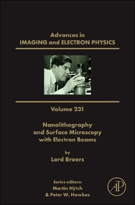
Nanolithography and Surface Microscopy with Electron Beams
Academic Press Inc (Verlag)
978-0-443-31462-9 (ISBN)
Peter Hawkes obtained his M.A. and Ph.D (and later, Sc.D.) from the University of Cambridge, where he subsequently held Fellowships of Peterhouse and of Churchill College. From 1959 – 1975, he worked in the electron microscope section of the Cavendish Laboratory in Cambridge, after which he joined the CNRS Laboratory of Electron Optics in Toulouse, of which he was Director in 1987. He was Founder-President of the European Microscopy Society and is a Fellow of the Microscopy and Optical Societies of America. He is a member of the editorial boards of several microscopy journals and serial editor of Advances in Electron Optics. Dr Martin Hÿtch, serial editor for the book series “Advances in Imaging and Electron Physics (AIEP), is a senior scientist at the French National Centre for Research (CNRS) in Toulouse. He moved to France after receiving his PhD from the University of Cambridge in 1991 on “Quantitative high-resolution transmission electron microscopy (HRTEM), joining the CNRS in Paris as permanent staff member in 1995. His research focuses on the development of quantitative electron microscopy techniques for materials science applications. He is notably the inventor of Geometric Phase Analysis (GPA) and Dark-Field Electron Holography (DFEH), two techniques for the measurement of strain at the nanoscale. Since moving to the CEMES-CNRS in Toulouse in 2004, he has been working on aberration-corrected HRTEM and electron holography for the study of electronic devices, nanocrystals and ferroelectrics. He was laureate of the prestigious European Microscopy Award for Physical Sciences of the European Microscopy Society in 2008. To date he has published 130 papers in international journals, filed 6 patents and has given over 70 invited talks at international conferences and workshops.
Introduction and Summary
Lord Broers
1. Early life
Lord Broers
2. Modification of an SEM/Ion beam system to improve the resolution and reliability of the SEM and remove oxygen ions from the ion beam
Lord Broers
3. Formation of cones and ridges on ion-etched surfaces
Lord Broers
4. Microfabrication in an SEM
Lord Broers
5. High Resolution Short Focal Length Lens Electron Probe
Lord Broers
6. Low-Loss Surface Microscopy in short focal length Probe
Lord Broers
7. Microfabrication in the 5Å electron probe
Lord Broers
8. Nanodevices fabricated in the HR Probe
Lord Broers
9. Fabrication of Structures with Dimensions Below 10 nm
Lord Broers
10. Semiconductor Lithography and Processing
Lord Broers
11. Nanolithography at 400kV
Lord Broers
12. Last twenty years and future of semiconductor chips
Lord Broers
| Erscheinungsdatum | 16.11.2024 |
|---|---|
| Reihe/Serie | Advances in Imaging and Electron Physics |
| Mitarbeit |
Herausgeber (Serie): Peter W. Hawkes, Martin Hÿtch |
| Verlagsort | San Diego |
| Sprache | englisch |
| Maße | 152 x 229 mm |
| Gewicht | 790 g |
| Themenwelt | Mathematik / Informatik ► Informatik |
| Technik ► Elektrotechnik / Energietechnik | |
| Technik ► Maschinenbau | |
| ISBN-10 | 0-443-31462-4 / 0443314624 |
| ISBN-13 | 978-0-443-31462-9 / 9780443314629 |
| Zustand | Neuware |
| Informationen gemäß Produktsicherheitsverordnung (GPSR) | |
| Haben Sie eine Frage zum Produkt? |
aus dem Bereich


