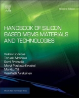
Handbook of Silicon Based MEMS Materials and Technologies
William Andrew Publishing (Verlag)
978-0-8155-1594-4 (ISBN)
- Titel erscheint in neuer Auflage
- Artikel merken
A comprehensive guide to MEMS materials, technologies and manufacturing, examining the state of the art with a particular emphasis on current and future applications.
Key topics covered include:
Silicon as MEMS material
Material properties and measurement techniques
Analytical methods used in materials characterization
Modeling in MEMS
Measuring MEMS
Micromachining technologies in MEMS
Encapsulation of MEMS components
Emerging process technologies, including ALD and porous silicon
Written by 73 world class MEMS contributors from around the globe, this volume covers materials selection as well as the most important process steps in bulk micromachining, fulfilling the needs of device design engineers and process or development engineers working in manufacturing processes. It also provides a comprehensive reference for the industrial R&D and academic communities.
Veikko Lindroos is Professor of Physical Metallurgy and Materials Science at Helsinki University of Technology, Finland.
Markku Tilli is Senior Vice President of Research at Okmetic, Vantaa, Finland.
Ari Lehto is Professor of Silicon Technology at Helsinki University of Technology, Finland.
Teruaki Motooka is Professor at the Department of Materials Science and Engineering, Kyushu University, Japan.
Markku Tilli obtained a degree in Materials Science (Physical Metallurgy) at Helsinki University of Technology (HUT) in 1974. Until 1980 he had various research and teaching positions at HUT specializing in crystal growth technologies. From 1981 to 1984 he managed process research and development in Silicon project at HUT silicon wafer manufacturing pilot plant. Since 1985 he has had various managing positions at Okmetic in research, development and customer support areas, and held a position of Senior Vice President, Research until his retirement in 2018. His MEMS related activities started in 1982 when he developed a process to make double side polished silicon wafers for bulk micromachined sensors. Since then he has developed advanced new silicon wafer types for MEMS, including special epitaxial wafers, SOI and SOI wafers with buried cavities. His publication topics include oxygen precipitation in silicon, silicon crystal growth, wafer cleaning as well as silicon wafer manufacturing technologies and applications in MEMS. He is member of the Technology Academy of Finland and has received the honorary degree of Doctor of Science in Engineering from Aalto University. Dr. Mervi Paulasto-Kröckel is professor at Aalto University School of Electrical Engineering in Finland. She studied materials science and semiconductor technology in Helsinki University of Technology, and gradudated as MSc Tech in 1990. She continued her studies in the Technical Universities of Aachen (RWTH Aachen) and Helsinki and attained her doctoral degree in 1995. After a 2-years post-doctoral appointment at the Joint Research Centre of European Commission in the Netherlands, her professional career continued in the electronics industry. She was a Staff Principal Engineer at Motorola Semiconductor Products Sector in Munich. In 2004 Paulasto-Kröckel joined Infineon Technologies where she was the Director Package Development responsible for semiconductor assembly and interconnect development for automotive products worldwide. At the end of 2018 Dr. Paulasto-Kröckel became a professor at Helsinki University of Technology, which is now called Aalto University after a merger with two other leading universities in the Helsinki area. Her current research focus is on advanced materials and interconnect technologies for MEMS/NEMS and power electronics, as well as multi-material assemblies behavior under different loads and their characteristic failure mechanisms. Her group has extensive experience in studying interactions and interfacial reactions between dissimilar materials, such as different oxide and nitride materials, metals and semiconductors. The group has developed a combined methodology approach to solve multi-materials compatibility issues in microelectronics and microsystems. Prof. Paulasto-Kröckel has over 110 international publications in the fields of microelectronics packaging and interfacial compatibility of dissimilar materials. She is IEEE EPS Distinguished Lecturer and a member of the Finnish Academy of Technical Sciences. Teruaki Motooka received PhD degree in 1981 in Applied Physics from Kyushu University. He was a research scientist in the Central Research Laboratory, Hitachi Ltd. for 1971-1984, a visiting research assistant professor at University of Illinois at Urbana-Champaign, USA for 1984-1988, an associate professor in the Institute of Applied Physics at University of Tsukuba, Japan for 1988-1993, and became a full professor at Kyushu University in 1993. He retired from Kyushu University in 2010. He has published more than 150 scientific papers on various international journals and these papers have been cited more than 2000 times. Veikko Lindroos is Professor Emeritus, Physical Metallurgy and Materials Science, Aalto University, Finland. His research covers a broad spectrum of materials science and technology, such as metallic materials, silicon technology and MEMS materials magnetic, electronic and composite materials as well as shape memory effect and materials.
PART I: Silicon as MEMS MaterialEdited by Markku Tilli1. Properties of silicon2. CZ Growth of silicon crystals3. Properties of silicon crystals4. Oxygen in Silicon5. Silicon wafers; preparation and properties6. Epi wafers; preparation and properties7. Thick-Film SOI wafers; preparation and properties8. Silicon dioxidesPART II: Modeling in MEMSEdited by Teruaki Motooka and Risto Nieminen9. Multiscale modeling methods10. Manufacture and processing of MEMS structures11. Mechanical properties of silicon microstructures12. Electrostatic and RF properties of MEMS structures13. Optical Modelling of MEMS 14. Gas Damping in Vibrating MEMS structuresPART III: Measuring MEMS Edited by Veli-Matti Airaksinen15. Introduction to Measuring MEMS16. Silicon wafer and thin film measurements17. Optical measurement of static and dynamic displacement18. MEMS residual stress characterization, methodology and perspective19. Strength of bonded interfaces20. Focused ion and electron beam techniques21.Oxygen and Bulk Microdefects in SiliconPART IV: Micromachining Technologies in MEMS Edited by Helmut Seidel22. MEMS litography23. Deep reactive ion etching (DRIE)24. Wet etching of silicon25. Porous silicon based MEMS26. Atomic layer deposition in MEMS technology27. Metallic glass29. Surface micromachining29. Silicon based bioMEMS micromachining technologiesPART V: Encapsulation of MEMS ComponentsEdited by Heikki Kuisma and Ari Lehto30. Introduction to encapsulation of MEMS devices31. Silicon direct bonding32. Anodic bonding33. Glass frit bonding34. Metallic alloy seal bonding35. Bonding CMOS processed wafers36. Non-Destructive Bond Strength Testing of Anodic Bonded Wafers37. Wafer Bonding Equipment38. Encapsulation by Film Deposition 39. Via Technologies for MEMS40. Outgassing and Gettering41. Dicing of MEMS devices42. Hermecity Tests
| Erscheint lt. Verlag | 22.2.2010 |
|---|---|
| Reihe/Serie | Micro and Nano Technologies |
| Verlagsort | Norwich |
| Sprache | englisch |
| Gewicht | 1730 g |
| Themenwelt | Technik ► Elektrotechnik / Energietechnik |
| Technik ► Maschinenbau | |
| ISBN-10 | 0-8155-1594-4 / 0815515944 |
| ISBN-13 | 978-0-8155-1594-4 / 9780815515944 |
| Zustand | Neuware |
| Haben Sie eine Frage zum Produkt? |
aus dem Bereich
