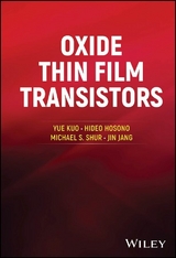
Oxide Thin Film Transistors (eBook)
391 Seiten
Wiley (Verlag)
978-1-394-20025-2 (ISBN)
Comprehensive resource reviewing fundamentals, device physics and reliability, fabrication processes, and numerous emerging applications of oxide thin film transistor technology over performing traditional thin film transistor technologies
Oxide Thin Film Transistors book presents a comprehensive overview of oxide thin film transistor (TFT) science and technology, including fundamental material properties, device operation principles, modeling, fabrication processes, and applications.
Split into four sections, the book first details oxide TFT materials including material parameters, and electrical and contact properties. The next section describes oxide TFT devices including designs, reliability, and comparison with other TFT types. The third part delves into the fabrication processes of oxide TFTs. The last section provides insight into existing and emerging applications of oxide TFTs including displays, imagers, circuits, sensors, flexible electronics, and circuits.
Written by a team of well-reputed researchers in the field including the inventor of the IGZO TFT, Oxide Thin Film Transistors include information on:
- Electronic and crystal structure of widegap oxides, covering electronic structure of n- and p-type oxide semiconductors as well as doping limit and band alignment
- Device physics, covering operation principles, reliability, comparison with other TFT types, and high-frequency performance
- Fabrication processes, covering deposition methods, gate insulators, and passivation layers
- Applications, covering liquid crystal, light emitting diode, and electrophoretic displays, flexible electronics, imagers, and integrated circuits
Oxide Thin Film Transistors is an ideal textbook resource for students who want to learn about oxide TFTs and a useful, up-to-date reference for researchers and engineers working on oxide TFTs and in related areas.
Yue Kuo is Life Chair Professor in the Photonics Department of National Yang Ming Chiao Tung University.
Hideo Hosono is an honorary and institute professor of Tokyo Institute of Technology.
Michael S. Shur is Patricia W. and C. Sheldon Roberts Professor of Solid State Electronics at Rensselaer Polytechnic Institute.
Jin Jang is a Chair Professor in the Department of Information Display of Kyung Hee University.
Comprehensive resource reviewing fundamentals, device physics and reliability, fabrication processes, and numerous emerging applications of oxide thin film transistor technology over performing traditional thin film transistor technologies Oxide Thin Film Transistors book presents a comprehensive overview of oxide thin film transistor (TFT) science and technology, including fundamental material properties, device operation principles, modeling, fabrication processes, and applications. Split into four sections, the book first details oxide TFT materials including material parameters, and electrical and contact properties. The next section describes oxide TFT devices including designs, reliability, and comparison with other TFT types. The third part delves into the fabrication processes of oxide TFTs. The last section provides insight into existing and emerging applications of oxide TFTs including displays, imagers, circuits, sensors, flexible electronics, and circuits. Written by a team of well-reputed researchers in the field including the inventor of the IGZO TFT, Oxide Thin Film Transistors include information on: Electronic and crystal structure of widegap oxides, covering electronic structure of n- and p-type oxide semiconductors as well as doping limit and band alignmentDevice physics, covering operation principles, reliability, comparison with other TFT types, and high-frequency performanceFabrication processes, covering deposition methods, gate insulators, and passivation layersApplications, covering liquid crystal, light emitting diode, and electrophoretic displays, flexible electronics, imagers, and integrated circuits Oxide Thin Film Transistors is an ideal textbook resource for students who want to learn about oxide TFTs and a useful, up-to-date reference for researchers and engineers working on oxide TFTs and in related areas.
1
Introduction of Metal Oxide Thin Film Transistors
1.1 Progress of Thin Film Transistor Development
The concept of the field effect transistor (FET) was originally proposed in 1925 and patented in 1926, as shown in Figure 1.1 [1, 2]. The thin film transistor (TFT) is operated on the same principle as that of the metal oxide field effect transistor (MOSFET). The first functional TFT, which had an evaporated microcrystalline (mc) CdS semiconductor channel layer and SiO gate dielectric with a staggered structure, was reported by Weimer in 1962 [3]. It was originally designed for electronic circuit applications [4]. Subsequently, various types of inorganic or organic semiconductor materials including tin oxide were made into TFTs [5, 6]. Originally, TFTs were aimed at circuit applications. However, they could not compete with the silicon wafer-based MOSFETs. New applications of TFTs were searched based on the advantageous low-temperature, low-temperature process capability. Brody et al. [7] first reported a 6″ by 6″ active matrix liquid crystal display (AMLCD) with a CdSe TFT array. It opened the high-performance flat panel era because the TFT could provide gray-scale switching capability for LC in each pixel and a TFT array could be prepared at a low temperature on a large-area substrate.
Figure 1.1 History of TFT and IC development.
Source: Kuo et al. [1]/John Wiley & Sons.
In the beginning, there were many efforts in mass production of AMLCDs using TFT backplates, but only limited success was achieved due to many manufacturing issues. However, the report of the amorphous silicon (a-Si:H) TFT by LeComber et al. [8] in 1979 provided a viable solution in manufacturing the large-area AMLCDs. It immediately attracted great attention from all electronics companies. The intrinsic a-Si:H channel, n+ ohmic contact layer, and gate dielectric in the TFT were all deposited by the plasma-enhanced chemical vapor deposition (PECVD) process. The low temperature process condition makes it possible to fabricate the large TFT array over a low-cost glass or even a plastic substrate. The gate dielectric and channel layers can be deposited by one-pump-down, which warrants the high performance and reliability of the TFT. The 10.4″ direct-view TFT LCD was included in the IBM ThinkPad PC in 1989. Other a-Si:H TFT-based products, such as X-ray medical imagers, gas, pH, photo, and magnetic sensors, were published in the literature [9]. Commercial 98″ TFT LCD TVs were available on the market in 2023 [10]. Glass substrates as large as 3 m by 3 m have been used in the 10.5th generation production equipment. The TFT LCD industry became the second largest electronic industry after the IC industry.
The main disadvantage of the a-Si:H TFT is the low field effect mobility (μeff), i.e., typically less than 1 cm2/V s. which limits its applications in high-speed or high driving-current products, such as the display driver circuit or the organic light-emitting diode (OLED). On the other hand, the polycrystalline silicon (poly-Si) thin film has been used as the gate electrode in MOSFETs since 1970s. It is natural for researchers to develop poly-Si TFTs from the early stage. The poly-Si TFT can have a mobility 2 orders of magnitude higher than that of the a-Si:H [11]. However, it is difficult to mass-produce poly-Si TFT arrays on a large-area substrate at a low temperature due to manufacturing reasons. The high-mobility poly-Si TFT is commonly made of high-temperature deposited poly-Si film or thermally annealed a-Si film, which is incompatible with the thermal stability of commercial display glass. The low thermal-budget laser annealing method, which provides the best poly-Si characteristics, suffers from low throughput. Therefore, currently, most poly-Si TFTs are used in small-sized displays.
Despite the early report of the high mobility SnO2 TFT, i.e., μeff = 70 cm2/V s, in 1964 [6], the metal oxide TFT was never used in commercial products until the report of the amorphous indium gallium zinc oxide (a-IGZO) TFT by the Hosono’s group in 2004 [12]. The renewed interest in industry and academia came from the possibility of mass production of the high μeff at a low temperature over a large-area substrate. The original a-IGZO TFT was made of the pulsed laser ablation deposition method at room temperature. The original large off-current (Ioff) was later reduced to <10−14 A [13]. Also, the complete TFT could be fabricated by the sputtering or PECVD process, which is suitable for the large-area, low-temperature, and high-throughput production requirements.
1.2 Progress of Metal Oxide Thin Film Transistor Development
Figure 1.2 shows a short summary of some important events related to metal oxide TFTs. For the rest of this book, the term “metal oxide TFT” will be shortened as “oxide TFT.” Shockley and Pearson first reported that the p-type semiconductor Cu2O could be used as a channel material for the FET 1948 [14]. The result remained at the current field modulation level and almost unchanged to date. Although several Cu+-based p-type oxide semiconductors, such as CuAlO2, have been reported, no good performance TFT has been reported so far [15]. In 1954, semiconducting oxide glasses based on V2Ox-P2O5 were reported by a group at Sheffield University [16]. This is the first report on the electronic conducting (bulk) glass, but the conduction is due to variable-range hopping between localized V4+ and V5+. Thus, this type of oxide semiconductor has very small mobility and cannot be used as the TFT channel material. Since then, it is well-known that transition metal oxides exhibit semiconducting properties. Transition metal cations have an open shell structure in their d-orbitals and give visible absorption originating from a d-d transition. Since these vacant d-levels give a large density of states (DOS) in the gap, it is hard to shift Fermi level (EF) significantly exceeding these DOS. This is the reason why transition metal oxide semiconductors do not work as TFT channel materials. Requirements on TFT channel semiconductor materials are much more severe than those for p-n junction formation because the EF has to shift to beyond the valence band maximum (VBM) or the conduction band minimum (CBM) upon the application of a gate voltage. High sensitivity of Cu+ to oxidation to Cu2+ at the surface and grain boundary [17] prevents the gate-bias-induced band conduction notwithstanding Cu2O thin films have high Hall mobility of ∼90 cm2/V s [17].
Figure 1.2 Examples of important events related to metal oxide TFTs.
Since the first report of the SnO2 TFT by Klasens and Koelmans at Philips Research Laboratories in 1964 [6], there have been many studies on oxide TFTs. In 1972, a study of the optical and electrical properties of Cd2SnO4 revealed its semiconductor properties [18]. In 1996, Hosono et al. [19] described the electrical properties of three transparent conducting amorphous oxides: a-AgSbO3, Cd2GeO4, and Cd2PbO4 having an electron mobility of ∼10 cm2/V s. This discovery was followed by the report on crystalline transparent oxide semiconductors [20] and by the report on the room-temperature fabrication of transparent flexible TFTs using amorphous oxide semiconductors [12]. In 2003, Hoffman et al. [21] reported on the ZnO-based transparent thin-film transistor.
Oxide TFT research was revisited extensively by several groups since 2000. A motivation was to develop TFTs with higher mobility and facile fabricability for next-generation flat panel displays (FPDs), such as OLEDs. Among them, noteworthy is a paper in 2001 by Ohya et al., which is the first report of a non-vacuum, solution process in preparing ZnO-TFTs, i.e., drop-coating of Zn(CH3COO)2 solution and subsequent heating in air [22]. Since high chemical stability in an ambient atmosphere is one of the material advantages of oxide semiconductors, this approach utilizing this intrinsic nature of oxides became a milestone in the fabrication of solution-derived oxide TFTs. Many papers on ZnO-TFTs deposited by sputtering or pulsed laser deposition were reported but serious issues, such as poor reproducibility and large hysteresis, arising mainly from the complex grain boundary nature, were pointed out. The design concept of transparent amorphous oxide semiconductors (TAOS) with large electron mobility was proposed by Hosono et al. [23] in 1996 along with several demonstrative materials. Although amorphous InOx had large electron mobility and high transparency, the performance of a-InOx TFTs was insufficient due to high carrier concentration [24]. A TAOS material, i.e., IGZO, appropriate for TFTs was found [12]. First, IGZO TFT was fabricated using epitaxial thin films of IGZO in 2003, exhibiting excellent performance, mobility of ∼80 cm2/V s and on- and off-current ratio (Ion/Ioff) of 106 [25]....
| Erscheint lt. Verlag | 1.11.2024 |
|---|---|
| Sprache | englisch |
| Themenwelt | Naturwissenschaften ► Chemie |
| Technik ► Maschinenbau | |
| Schlagworte | oxide TFT applications in displays, imagers, sensors, flexible electronics, and circuits • oxide TFT designs • oxide TFT devices • oxide TFT electrical properties • oxide TFT fabrication processes • oxide TFT materials • oxide TFT reliability • TFTs |
| ISBN-10 | 1-394-20025-0 / 1394200250 |
| ISBN-13 | 978-1-394-20025-2 / 9781394200252 |
| Informationen gemäß Produktsicherheitsverordnung (GPSR) | |
| Haben Sie eine Frage zum Produkt? |
Größe: 31,8 MB
Kopierschutz: Adobe-DRM
Adobe-DRM ist ein Kopierschutz, der das eBook vor Mißbrauch schützen soll. Dabei wird das eBook bereits beim Download auf Ihre persönliche Adobe-ID autorisiert. Lesen können Sie das eBook dann nur auf den Geräten, welche ebenfalls auf Ihre Adobe-ID registriert sind.
Details zum Adobe-DRM
Dateiformat: EPUB (Electronic Publication)
EPUB ist ein offener Standard für eBooks und eignet sich besonders zur Darstellung von Belletristik und Sachbüchern. Der Fließtext wird dynamisch an die Display- und Schriftgröße angepasst. Auch für mobile Lesegeräte ist EPUB daher gut geeignet.
Systemvoraussetzungen:
PC/Mac: Mit einem PC oder Mac können Sie dieses eBook lesen. Sie benötigen eine
eReader: Dieses eBook kann mit (fast) allen eBook-Readern gelesen werden. Mit dem amazon-Kindle ist es aber nicht kompatibel.
Smartphone/Tablet: Egal ob Apple oder Android, dieses eBook können Sie lesen. Sie benötigen eine
Geräteliste und zusätzliche Hinweise
Buying eBooks from abroad
For tax law reasons we can sell eBooks just within Germany and Switzerland. Regrettably we cannot fulfill eBook-orders from other countries.
aus dem Bereich


