Photo-induced Defects in Semiconductors
Seiten
2006
Cambridge University Press (Verlag)
978-0-521-02445-7 (ISBN)
Cambridge University Press (Verlag)
978-0-521-02445-7 (ISBN)
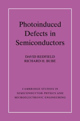
This is the first book to give a complete overview of the properties of deep-level, localized defects in semiconductors. These metastable defects exhibit complex interactions with the surrounding material, and can significantly affect the performance and stability of certain semiconductor devices.
This is the first book to give a complete overview of the properties of deep-level, localized defects in semiconductors. Such comparatively long-lived (or metastable) defects exhibit complex interactions with the surrounding material, and can significantly affect the performance and stability of certain semiconductor devices. After an introductory discussion of metastable defects, the properties of DX and EL2 centres in III–V compounds are presented. Additional crystalline materials are also dealt with, before a detailed description is given of the properties and kinetics of photo-induced defects in amorphous semiconductors. The book closes with an examination of the effects of photo-induced defects in a range of practical applications. Throughout, unifying concepts and models are stressed, and the book will be of great use to graduate students and researchers interested in the physics and materials science of semiconductors.
This is the first book to give a complete overview of the properties of deep-level, localized defects in semiconductors. Such comparatively long-lived (or metastable) defects exhibit complex interactions with the surrounding material, and can significantly affect the performance and stability of certain semiconductor devices. After an introductory discussion of metastable defects, the properties of DX and EL2 centres in III–V compounds are presented. Additional crystalline materials are also dealt with, before a detailed description is given of the properties and kinetics of photo-induced defects in amorphous semiconductors. The book closes with an examination of the effects of photo-induced defects in a range of practical applications. Throughout, unifying concepts and models are stressed, and the book will be of great use to graduate students and researchers interested in the physics and materials science of semiconductors.
1. Introduction: metastable defects; 2. III–V compounds: DX2 and EL2 centers; 3. Other crystalline materials; 4. Hydrogenated amorphous silicon: properties of defects; 5. Hydrogenated amorphous silicon: photo-induced defect kinetics and processes; 6. Other amorphous semiconductors; 7. Photo-induced defect effects in devices; References; Index.
| Erscheint lt. Verlag | 9.3.2006 |
|---|---|
| Reihe/Serie | Cambridge Studies in Semiconductor Physics and Microelectronic Engineering |
| Zusatzinfo | 1 Halftones, unspecified; 105 Line drawings, unspecified |
| Verlagsort | Cambridge |
| Sprache | englisch |
| Maße | 152 x 229 mm |
| Gewicht | 350 g |
| Themenwelt | Naturwissenschaften ► Physik / Astronomie ► Elektrodynamik |
| Technik ► Elektrotechnik / Energietechnik | |
| ISBN-10 | 0-521-02445-5 / 0521024455 |
| ISBN-13 | 978-0-521-02445-7 / 9780521024457 |
| Zustand | Neuware |
| Haben Sie eine Frage zum Produkt? |
Mehr entdecken
aus dem Bereich
aus dem Bereich
eine Einführung in die Gleich- und Wechselstromtechnik
Buch | Hardcover (2024)
Hanser (Verlag)
34,99 €
Grundlagen und praktische Anwendungen
Buch | Hardcover (2022)
Hanser (Verlag)
34,99 €


