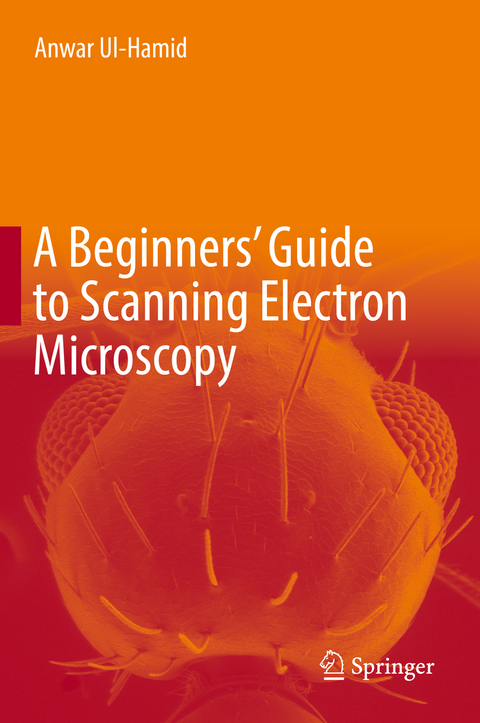
A Beginners' Guide to Scanning Electron Microscopy
Springer International Publishing (Verlag)
978-3-319-98481-0 (ISBN)
- provides a concise and accessible introduction to the essentials of SEM
- includes a large number of illustrations specifically chosen to aid readers' understanding of key concepts
- highlights recent advances in instrumentation, imaging and sample preparation techniques
- offers examples drawn from a variety of applications that appeal to professionals from diverse backgrounds.
Anwar Ul-Hamid received his B.Sc. in Metallurgical Engineering and Materials Science at the University of Engineering & Technology in Lahore, Pakistan in 1991. He received his Ph.D,. for Oxidation of High Temperature alloys/Analytical Electron Microscopy at the Department of Materials Science & Metallurgy at the University of Cambridge in 1996. He has published over 70 peer-reviewed papers in journals and proceedings, and is currently Coordinator of the Materials Characterization Laboratory (MCL)/Research Institute at King Fahd University of Petroleum & Minerals, in Dhahran, Saudi Arabia.
Introduction.- What is the SEM.- Image Resolution in the SEM.- Image Formation in the SEM.- Information obtained using the SEM.- Brief History of the SEM Development.- Components of the SEM.- Primary Components.- Electron Column.- Electron Gun.- Thermionic Emission Electron Guns.- Tungsten Filament Guns.- Lanthalum Hexaboride (LaB6) Emitter Guns.- Field Emission Electron Guns.- Electromagnetic Lenses.- Condenser Lenses.- Objective Lenses.- Pinhole Lens.- Immersion Lens.- Snorkel Lens.- Lens Aberrations.- Spherical Aberration.- Chromatic Aberration.- Astigmatism.- Scan Coils.- Objective Aperture.- Specimen Chamber.- Specimen Stage.- CCD Camera.- Detectors.- Secondary Electron Detector (SED).- Backscattered Electron Detector (BSED).- Energy Dispersive X-ray Spectrometer (EDS Detector).- Low Vacuum Detector.- Low Voltage High Contrast Detector.- Through-the-lens Detector.- Electron Backscattered Diffraction (EBSD) Detector.- Scanning Transmission Electron Microscopy (STEM) Detector.- Computer Control System.- Secondary Components.- Vacuum System.- Chiller.- Heater.- Electronics.- Anti-Vibration Platform.- Specialized Equipment.- Focused Ion Beam (FIB) Instrument.- Combined Focused Ion Beam-Scanning Electron Microscope.- Beam-Specimen Interaction.- Atom Model.- Elastic Scattering.- Inelastic Scattering.- Effect of Electron Scattering.- Interaction Volume.- Electron Range.- Signals Obtained From the Specimen.- Backscattered Electrons.- Secondary Electrons.- Characteristic X-Ray Lines.- White Radiation.- X-Ray Fluorescence.- Cathodoluminescence Radiation.- Imaging with the SEM.- Image Formation in the SEM.- Magnification.- Resolution.- Depth of Field.- Contrast.- Secondary Electron Imaging.- Backscattered Electron Imaging.- Influence of Various Factors on SEM Imaging.- Effect of Accelerating Voltage.- Effect of Probe Current.- Effect of Working Distance.- Effect of Objective Aperture.- Effect of Tilt.- Astigmatism.- Image Distortion.- Incorrect Alignment.- Beam Damage.- Charging.- Edge Effect.- Sample direction with respect to the Detector Position.- Factors affecting Image Quality: Indications-Causes-Remedies.- Summary of Specialized Imaging Techniques.- Imaging at Low Vacuum.- Imaging at Low Voltage.- Environmental SEM.- Imaging at Low/Elevated Temperature.- Imaging Samples under Stress.- Use of Tilt and Rotation during Imaging.- Use of STEM detector in SEM.- Use of EBSD in SEM.- SEM Operation.- Specimen Insertion.- Image Acquisition.- Microscope Alignment.- Image Quality.- High Resolution Imaging.- Maintenance of the SEM.- Microchemical Analysis with the SEM.- Working of the EDS Detector.- Characteristics of the EDS Detector.- Qualitative EDS Analysis.- Quantitative EDS Analysis.- Atomic Number (Z) Effect.- X-ray Absorption (A) Effect.- X-ray Fluorescence (F) Effect.- ZAF Corrections.- Standardless Analysis.- Trace Element Analysis.- Sample Preparation.- Metals, Alloys, Ceramics and Semiconductors.- Polymers.- Geological Samples.- Biological Samples.- Semiconductors.- Use of Focused Ion Beam.
| Erscheinungsdatum | 14.11.2018 |
|---|---|
| Zusatzinfo | XXII, 402 p. 220 illus., 98 illus. in color. |
| Verlagsort | Cham |
| Sprache | englisch |
| Maße | 155 x 235 mm |
| Gewicht | 795 g |
| Themenwelt | Technik ► Maschinenbau |
| Schlagworte | components of the SEM • sample preparation for SEM • Scanning Electron Microscopy • SEM instrumentation • Specialized imaging techniques • theory of specimen-beam interaction |
| ISBN-10 | 3-319-98481-0 / 3319984810 |
| ISBN-13 | 978-3-319-98481-0 / 9783319984810 |
| Zustand | Neuware |
| Informationen gemäß Produktsicherheitsverordnung (GPSR) | |
| Haben Sie eine Frage zum Produkt? |
aus dem Bereich


