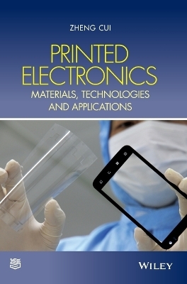
Printed Electronics
John Wiley & Sons Inc (Verlag)
978-1-118-92092-3 (ISBN)
Provides an overview of the latest developments and research results in the field of printed electronics
Topics addressed include: organic printable electronic materials, inorganic printable electronic materials, printing processes and equipments for electronic manufacturing, printable transistors, printable photovoltaic devices, printable lighting and display, encapsulation and packaging of printed electronic devices, and applications of printed electronics
Discusses the principles of the above topics, with support of examples and graphic illustrations
Serves both as an advanced introductory to the topic and as an aid for professional development into the new field
Includes end of chapter references and links to further reading
Prof Zheng Cui, Chinese Academy of Sciences, China Zheng Cui obtained a PhD in electronic engineering in 1988 and became a Visiting Fellow at the Microelectronics Research Center, Cambridge University, UK, in 1989. Cui joined the Rutherford Appleton Laboratory, UK, in 1993 and subsequently became a Principal Scientist and group leader there in 1999. In October 2009, after working in the UK for 20 years, Cui returned to China and founded the Printable Electronics Research Center at the Suzhou Institute of Nanotech, which was the first research center dedicated to printed electronics R&D in China. CONTRIBUTORS Dr Song Qiu, Chinese Academy of Sciences, China Song Qiu received a B.S. Polymer Materials and Engineering in 2000, followed by a PhD in Polymer Chemistry and Physics?from Jilin University in 2005. Dr Jian Lin, Chinese Academy of Sciences, China Jian Lin received his PhD degree in Polymer Chemistry and Physics from Changchun Institute of Applied Chemistry, Chinese Academy of Sciences in 2008. Dr. Jianwen Zhao, Chinese Academy of Sciences, China Jianwen Zhao received his PhD degree in Technical Institute of Physics and Chemistry, Chinese Academic of Science, in 2008. Dr. Chang-Qi Ma, Chinese Academy of Sciences, China Chang-Qi Ma received his bachelor's degree in Chemistry from Beijing Normal University in 1998. In 2003 he obtained his PhD degree at the Technical Institute of Physics and Chemistry, Chinese Academy of Sciences in Beijing with Professor B.-W. Zhang. Dr. Zheng Chen, Chinese Academy of Sciences, China Zheng Chen received the B.S. degree in materials physics and PhD degree in condensed matter physics from the University of Science and Technology of China, in 2002 and 2007, respectively. Dr. Wenming Su, Chinese Academy of Sciences, China Wenming Su is anAssociate professor of Printable Electronics Research Center, Suzhou Institute of Nanotech, Chinese Academy of Sciences.
Preface xii
1 Introduction 1
Zheng Cui
1.1 What is Printed Electronics? 1
1.2 The Importance of Developing Printed Electronics 11
1.3 Multidisciplinary Nature of Printed Electronics 15
1.4 Structure and Content of the Book 17
References 19
2 Organic Printable Electronic Materials 21
Song Qiu and Chunshan Zhou
2.1 Introduction 21
2.2 Organic Conductive Materials 22
2.2.1 Characteristics of Organic Conductive Materials 22
2.2.2 History of Organic Conductive Materials 23
2.2.3 Conductive Polymer 23
2.2.3.1 Structural Conductive Polymer 23
2.2.3.2 Composite Conductive Polymer 25
2.2.4 PEDOT 25
2.3 Printable Organic Small Molecular Semiconductors 27
2.3.1 Fused Aromatic Compounds 28
2.3.2 Heterocyclic Sulfur Compounds and Oligothiophenes 30
2.3.3 Other Materials with High Mobility 33
2.4 Printable Polymeric Semiconductor 34
2.4.1 P‐type Polymer Semiconductors 35
2.4.1.1 Sulfur‐containing Heterocyclic Polymeric Semiconductors 35
2.4.1.2 Phenyl‐containing Polymeric Semiconductors 37
2.4.1.3 Other p‐type Polymeric Semiconductors 39
2.4.2 N‐type Polymer Semiconductors 39
2.4.3 Ambipolar Transistor and Related Polymer Materials 41
2.4.4 Outlook 43
2.5 Other Printable Organic Electronic Materials 44
2.5.1 Organic Insulating Materials 44
2.5.2 Organic Materials for Sensors 47
2.6 Summary 49
References 49
3 Inorganic Printable Electronic Materials 54
Zheng Chen
3.1 Introduction 54
3.2 Metallic Materials 56
3.2.1 Metallic Ink 56
3.2.2 Post‐printing Process 63
3.2.3 Metal Nanowire 64
3.3 Transparent Oxide 66
3.3.1 Transparent Oxide Semiconductor and Conductor 66
3.3.2 Low Temperature Solution Processing 68
3.3.3 Doped Transparent Oxide Nanoparticles 71
3.4 Single‐wall Carbon Nanotube 72
3.4.1 Preparation and Selective Chemistry of SWNT 72
3.4.2 Purification of SWNT 76
3.4.3 Metallic SWNT Thin Film 77
3.4.4 Semiconducting SWNT Thin Film 79
3.5 Graphene 83
3.6 Silicon and Germanium 86
3.7 Metal Chalcogenides Semiconductor and Quantum Dots 90
3.7.1 Metal Chalcogenides Semiconductor 90
3.7.2 Quantum Dots 90
3.8 Nanoparticle/Polymer Dielectric Composites 92
3.9 Summary 95
References 96
4 Printing Processes and Equipments 106
Jian Lin
4.1 Introduction 106
4.2 Jet Printing 108
4.2.1 Inkjet Printing 108
4.2.1.1 Working Principles 108
4.2.1.2 Pattern Preparation 108
4.2.1.3 Application in Printed Electronics 110
4.2.2 Aerosol Jet Printing 111
4.2.2.1 Working Principle 112
4.2.2.2 Pattern Preparation 112
4.2.2.3 Advantages and Challenges 113
4.2.3 Electrohydrodynamic Jet Printing 114
4.2.4 Advantages and Disadvantages 114
4.3 Direct Replicate Printing 115
4.3.1 Screen Printing 116
4.3.1.1 Working Principle 116
4.3.1.2 Screen Mask 117
4.3.1.3 Advantages and Disadvantages 118
4.3.1.4 Applications 118
4.3.2 Gravure Printing 118
4.3.2.1 Principle and System 118
4.3.2.2 Gravure Plate 120
4.3.2.3 Advantages and Disadvantages 120
4.3.2.4 Applications in Printed Electronics 121
4.3.3 Flexographic Printing 122
4.3.3.1 Principle and System 122
4.3.3.2 Printing Plate 123
4.3.3.3 Advantages and Disadvantages 123
4.3.3.4 Applications in Printed Electronics 125
4.4 Indirect Replicate Printing 125
4.4.1 Offset Printing 125
4.4.2 Gravure Offset Printing 126
4.4.3 Pad Printing 128
4.5 Pre‐printing Processes 129
4.5.1 Pattern Design 129
4.5.2 Modification of Surface Energy 130
4.5.3 Surface Coating 131
4.5.4 Embossing and Nanoimprinting 131
4.6 Post‐printing Processes 134
4.6.1 Sintering 134
4.6.2 UV Curing 135
4.6.3 Annealing 135
4.7 Summary 136
References 137
5 Printed Thin Film Transistors 145
Jianwen Zhao
5.1 Introduction 145
5.2 Types of Transistors 146
5.3 Working Principles of Transistors 147
5.3.1 Basic Mechanism of MOSFETs 147
5.3.2 Charge Carriers and Carrier Mobility 149
5.3.3 Basic Parameters of TFT 149
5.3.3.1 Effective Mobility 149
5.3.3.2 Operating Voltage 151
5.3.3.3 Device Capacitance 151
5.3.3.4 Threshold Voltage (Vt) 153
5.3.3.5 Subthreshold Swing (SS) 155
5.3.3.6 On/off Current Ratio (Ion /Ioff) 155
5.3.3.7 Hysteresis 156
5.3.3.8 Transconductance (gm) 157
5.3.3.9 Stability 157
5.4 Structures and Fabrication of TFTs 157
5.4.1 Structures of TFTs 157
5.4.2 Characteristics of TFTs 159
5.4.3 Fabrication of TFTs 160
5.4.3.1 Fabrication of Electrodes 160
5.4.3.2 Fabrication of Active Layer 163
5.4.3.3 Fabrication of Dielectric Layers 167
5.5 Fully Printed TFTs 172
5.5.1 Printability of Electronic Materials 172
5.5.2 Influence of Surface Morphology 173
5.5.3 Interface Effect of Printed TFTs 173
5.5.3.1 Effect of Semiconductor/Dielectric Interface 175
5.5.3.2 Effect of Semiconductor/Semiconductor Interface 176
5.5.3.3 Effect of Semiconductor/Electrode Interface 177
5.5.4 Effect of Channel Length 178
5.5.5 Summary of Issues in Printing TFTs 179
5.5.5.1 Printable Inks and Printing Processes 179
5.5.5.2 Printed Electrodes 180
5.5.5.3 Printed Dielectric Thin Films 180
5.6 Advances in Printed TFTs 180
5.6.1 Printed Inorganic TFTs 181
5.6.1.1 SWCNT TFTs 181
5.6.1.2 Metal Oxide TFTs 182
5.6.1.3 Metal Dichalcogenide and Graphene TFTs 184
5.6.2 Printed Organic TFTs 187
5.7 Basics of Printed Logic Circuits 189
5.7.1 NAND and NOR Gates 190
5.7.2 Inverter 190
5.7.3 Ring Oscillator 190
5.7.4 Flip‐flop 193
5.7.5 Backplane Driving Circuits for Display 194
5.8 Summary 196
References 197
6 Printed Organic Thin Film Solar Cells 201
Changqi Ma
6.1 Introduction 201
6.1.1 Solar Energy and its Utilization 201
6.1.2 Classification of Solar Cells 202
6.1.3 A Brief History of Organic Thin‐Film Solar Cells 203
6.2 Working Principles and Characterization of Organic Solar Cells 205
6.2.1 Physical Processes 205
6.2.2 Basic Structure 206
6.2.3 Characterization 208
6.2.3.1 I‐V Characteristics 208
6.2.3.2 Spectrum Response 209
6.2.4 The Main Factors Influencing Device Performance 209
6.2.4.1 Photon Absorption Ability of Organic Semiconductors 210
6.2.4.2 Energy Level Arrangement of Donor and Acceptor 210
6.2.4.3 Morphology of Photoactive Layer 212
6.3 Materials for Organic Solar Cells 213
6.3.1 Transparent Substrate 214
6.3.2 Transparent Conductive Electrode 214
6.3.2.1 Metal Oxide Film 214
6.3.2.2 Conductive Polymer Film 215
6.3.2.3 Thin Metal Film and Metal Grid 215
6.3.2.4 Carbon‐rich Materials 217
6.3.3 Organic Semiconductor Materials 218
6.3.3.1 p‐Type Organic Semiconductors 218
6.3.3.2 n‐Type Organic Semiconductors 223
6.3.4 Inorganic Semiconductors 227
6.3.5 Other Functional Materials 229
6.4 Inverted and Tandem Organic Solar Cells 229
6.4.1 Inverted Organic Solar Cells 229
6.4.2 Tandem Organic Solar Cells 231
6.4.3 Inverted Tandem Organic Solar Cells 231
6.5 Fabrication Methods 232
6.5.1 Spin Coating 233
6.5.2 Doctor Blading 235
6.5.3 Screen Printing 235
6.5.4 Inkjet Printing 237
6.5.5 Other Thin Film Deposition Techniques 237
6.6 Roll‐to‐roll Processing 237
6.7 Printable Perovskite Solar Cells 239
6.8 Summary and Outlook 239
References 240
7 Printed Organic Light Emission and Display 251
Wenming Su
7.1 Introduction 251
7.1.1 Overview of Lighting and Display 252
7.1.2 Overview of Organic Light Emitting Diodes (OLEDs) 253
7.2 Mechanism of Organic Light Emission 254
7.2.1 Charge Injection and Transport 255
7.2.2 Exciton Formation and Light Emission 256
7.2.3 Characterization of OLED Performance 256
7.2.3.1 Luminous Efficacy 256
7.2.3.2 Quantum Efficiency 257
7.2.3.3 Color 257
7.2.3.4 Three Primary Colors 258
7.3 Structures and Materials of OLED 259
7.3.1 Small Molecular OLED 259
7.3.1.1 Typical Structure 259
7.3.1.2 Electrode Materials 259
7.3.1.3 Fabrication Process 260
7.3.2 Polymer OLEDs 262
7.3.3 General OLED Materials 262
7.3.3.1 Charge Injection Materials 263
7.3.3.2 Charge Transport Materials 263
7.3.3.3 Emitter Materials 264
7.3.4 Soluble OLED Materials 265
7.3.4.1 Printable Polymer OLEDs 266
7.3.4.2 Printable Small Molecular OLEDs 266
7.3.4.3 Cross‐linking Materials for Printable OLEDs 267
7.4 White Lighting OLEDs 267
7.4.1 White Light Emission Mechanism 267
7.4.2 Important Parameters 272
7.4.2.1 CRI 272
7.4.2.2 Efficiency and Light Extraction 273
7.4.2.3 Lifetime 275
7.4.3 Investment in OLED Lighting 275
7.5 Fabrication of OLED by Printing 277
7.5.1 Spin and Slot Die Coating 277
7.5.2 Inkjet Printing 278
7.5.3 Screen Printing 278
7.5.4 Roll‐to‐roll Printing 279
7.5.5 Current Status of the Printed OLED Industry 280
7.6 Summary 281
References 282
8 Encapsulation Technology for Organic Electronic Devices 287
Wenming Su
8.1 Introduction 287
8.2 Aging of Organic Electronic Devices 288
8.2.1 Characteristics and Mechanisms of Aging 288
8.2.2 Requirements for Organic Electronics Encapsulation 290
8.3 Principle of Encapsulation 291
8.3.1 Water/oxygen Penetration Mechanism through Thin Films 291
8.3.2 Organic/inorganic Multilayer Encapsulation 292
8.3.3 Measurement of Encapsulation Property 293
8.4 Thin‐film Encapsulation Technology 296
8.4.1 History of Thin‐film Encapsulation 297
8.4.2 Single Layer Thin‐film Encapsulation 298
8.4.3 Multilayer Thin‐film Encapsulation 298
8.4.4 BarixTM Thin‐film Encapsulation 300
8.4.5 Thin Film Deposition Methods 301
8.4.5.1 PECVD 301
8.4.5.2 ALD 303
8.4.5.3 Parylene Deposition 303
8.4.6 Flexibility of Encapsulation Thin Film 304
8.4.7 Trends of Thin‐film Encapsulation 306
8.5 Applications of Thin‐film Encapsulation 307
8.5.1 Encapsulation of Flexible OLED 307
8.5.2 Encapsulation of Flexible OPV 309
8.6 Summary 313
References 314
9 Applications and Future Prospects of Printed Electronics 316
Zheng Cui
9.1 Introduction 316
9.2 Application Areas of Printed Electronics 317
9.2.1 Organic Photovoltaic 317
9.2.2 Flexible Display 321
9.2.3 Organic Lighting 324
9.2.4 Electronics and Components 326
9.2.5 Integrated Smart Systems 331
9.3 Challenges for Printed Electronics 333
9.3.1 Materials 333
9.3.2 Printing Process and Equipment 335
9.3.3 Encapsulation 335
9.3.4 Design Methodology and Standardization 336
9.4 Summary and Outlook 336
References 337
Index 339
| Erscheinungsdatum | 28.05.2016 |
|---|---|
| Verlagsort | New York |
| Sprache | englisch |
| Maße | 163 x 246 mm |
| Gewicht | 680 g |
| Themenwelt | Technik ► Elektrotechnik / Energietechnik |
| Technik ► Maschinenbau | |
| Schlagworte | Communication technology • Electrical & Electronics Engineering • Electronic materials • Elektronische Materialien • Elektrotechnik u. Elektronik • Kommunikationstechnik • Materials Science • Materialwissenschaften |
| ISBN-10 | 1-118-92092-9 / 1118920929 |
| ISBN-13 | 978-1-118-92092-3 / 9781118920923 |
| Zustand | Neuware |
| Haben Sie eine Frage zum Produkt? |
aus dem Bereich


