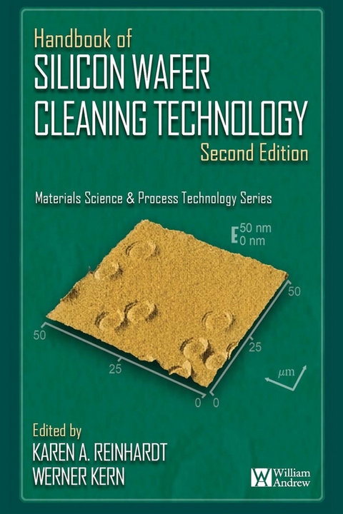
Handbook of Silicon Wafer Cleaning Technology (eBook)
660 Seiten
Elsevier Science (Verlag)
978-0-8155-1773-3 (ISBN)
• Focused on silicon wafer cleaning techniques including wet, plasma, and other surface conditioning techniques used to manufacture integrated circuits.
• As this book covers the major technologies for removing contaminants, it is a reliable reference for anyone that manufactures integrated circuits, or supplies the semiconductor and microelectronics industries.
• Covers processes and equipment, as well as new materials and changes required for the surface conditioning process.
• Editors are two of the top names in the field and are both extensively published.
• Discusses next generation processing techniques including supercritical fluid, laser, and cryoaerosol.
The second Edition of the Handbook of Silicon Wafer Cleaning Technology is intended to provide knowledge of wet, plasma, and other surface conditioning techniques used to manufacture integrated circuits. The integration of the clean processes into the device manufacturing flow will be presented with respect to other manufacturing steps such as thermal, implant, etching, and photolithography processes. The Handbook discusses both wet and plasma-based cleaning technologies that are used for removing contamination, particles, residue, and photoresist from wafer surfaces. Both the process and the equipment are covered. A review of the current cleaning technologies is included. Also, advanced cleaning technologies that are under investigation for next generation processing are covered; including supercritical fluid, laser, and cryoaerosol cleaning techniques. Additionally theoretical aspects of the cleaning technologies and how these processes affect the wafer is discussed such as device damage and surface roughening will be discussed. The analysis of the wafers surface is outlined. A discussion of the new materials and the changes required for the surface conditioning process used for manufacturing is also included. - Focused on silicon wafer cleaning techniques including wet, plasma, and other surface conditioning techniques used to manufacture integrated circuits- As this book covers the major technologies for removing contaminants, it is a reliable reference for anyone that manufactures integrated circuits, or supplies the semiconductor and microelectronics industries- Covers processes and equipment, as well as new materials and changes required for the surface conditioning process- Editors are two of the top names in the field and are both extensively published- Discusses next generation processing techniques including supercritical fluid, laser, and cryoaerosol
2 Overview of Wafer Contamination and Defectivity
Twan Bearda
IMEC, Ultra Clean Processing, Leuven, Belgium
Paul W. Mertens
IMEC, Ultra Clean Processing, Leuven, Belgium
Stephen P. Beaudoin
Purdue University, School of Chemical Engineering, West Lafayette, IN, USA
2.1 Wafer Contamination
This chapter provides an overview of the types of contamination and defects that are encountered during integrated circuit (IC) manufacturing and discusses their detrimental effects. Also discussed is how to balance the cleaning process to optimally remove the unwanted contamination and not contribute to undesired defectivity. The contamination encountered during the manufacturing process is present on the wafer, in the clean-room, or in the process chemicals and water. The criterion for a substance to be considered a contaminant is that it causes uncontrolled variations in the electrical performance of the device or in the device fabrication process. The contamination and defects may be observed visually or may only be detected with sophisticated analytical equipment during the inspection process or at the final device test.
According to the above definition, some (but not all) contaminants and defects have an impact on device performance. If the contamination causes a device to function improperly under predefined conditions, the contamination is said to have induced an electrical failure or defect on the integrated circuit (IC). Each failure detracts from the overall performance of the finished IC device, and a high frequency of failures can lead to a non-functioning IC device. It is important to note that defects may have other causes than contamination, such as poorly tuned process conditions or unexpected process variations. In this chapter, only defects that are related to contamination and defects that are unwillingly introduced by cleaning will be considered.
2.1.1 Classification of contamination and defects
It is possible to distinguish between groups of contaminants and defe cts that have similar behavior. Such a classification helps in organizing contamination control, but it should be noted that several classification schemes exist and every scheme has its limitations. This chapter will follow the conventional classification of contamination, which is largely based on detection methods. Also discussed in this chapter are several alternative classifications of defectivity.
2.1.1.1 Classification according to detection method
Many analytical tools are available to detect the presence of contamination. Chapters 8 and 10 discuss the methods for detecting particles on the surface of the wafer and in chemicals and H2O. The following types of contaminants are classified in this chapter according to the analytical techniques discussed in these chapters:
Metallic contamination: contamination consisting of (or containing) metallic species. Although the effect on devices may be dramatically different, usually for in-line monitoring no distinction is made between the different forms in which the contamination can be present (i.e. as an oxide, a silicide, pure metal, etc.). Common methods for detecting metallic contamination are total reflection X-ray fluorescence (TXRF), atomic absorption spectrometry (AA), and inductively coupled plasma–mass spectrometry (ICP-MS).
Particle contamination: contamination that is usually observed using light scattering tools. For this reason, a more correct name is “light-point defects“ (LPD). Recently it has become possible to distinguish between substrate defects that scatter light (crystal originated particles or pits, COP) and actual material deposits. In this chapter, the term “particles“ refers to the latter type of contamination.
Organic contamination: contamination containing a large amount of C or slight amount of C on the surface, plus the bonding structure associated with the C. One method for detecting surface contamination is thermal desorption–MS, other methods include X-ray photoelectron spectroscopy and Auger electron spectroscopy (AES).
Surface defectivity: defectivity associated with roughness of the Si and film surface or line edge roughness. Typically, atomic force microscopy (AFM) and associated techniques are used.
Atmospheric molecular contamination (AMC) and moisture: contamination that has molecular dimensions and can therefore not be removed with normal HEPA (high-efficiency particle air) or ULPA (ultra-low penetration air) filters. AMC is usually monitored with ion mass spectrometry and capillary electrophoresis.
Some contaminants may fall in more than one category. For example, particles may consist of either organic or metallic material, or contain both, and thus arbitrarily be classified as particulate, metallic or organic contamination. Figure 2.1-1 shows the effects of metallic compound particles with a density of 5 g/cm3 and a molecular mass of 100 amu (atomic mass unit) on the average metal concentration in atoms/cm2 on a 300-mm wafer. As can be seen, a high concentration of metals on the wafer surface an result either from large numbers of small particles or from small numbers of large particles. As a result, to minimize particle-derived metal contamination on wafers, both the size and number of contaminant particles must be minimized.
Figure 2.1-1 The effects of particle count and size on the equivalent metal concentration on a Si wafer surface.
Used with permission from authors.
2.1.1.2 Classification according to material
Recent years have seen a diversification of materials that are used in the fabrication of IC devices. Initially, the materials were limited to Si and the dopants necessary to control the semiconducting properties, SiO2-based insulation layers, Si3 N4 barriers, and sacrificial layers. For interconnect metallization, Al or Al/Cu alloys were used. Metal silicides were introduced to lower contact resistance. Later, TiN barriers and W plugs were used followed by Cu metallization and low-κ (low dielectric constant) dielectrics. Metallic oxides and metal gate electrodes replaced the memory cell and the transistor. While the use of these materials improves device performance, their presence in sensitive device regions can have a negative impact, as it takes only a very small number of metal atoms to dramatically change the electrical properties of device structures. Many metal atoms diffuse very rapidly through both Si and SiO2 layers, which highlights the importance of controlling metal contamination during device level processing and maintaining barrier integrity during interconnect processing. Therefore, rather than being based on the detection method, a classification system may be based on the contaminant composition. In general, the contamination may be similar or dissimilar to the substrate material. This has important consequences for the cleaning method that is to be used to remove the contamination.
If the contamination consists of a different material than the substrate then it can, in principle, be removed by a material-selective cleaning method. Such methods may involve selective dissolution of the contaminant, selective dissolution of the substrate surrounding the contaminant, chelation of the contaminant, solution modification to create repulsion between the contaminant and substrate, or chemical reaction to convert the contaminant to a soluble or volatile product. This “chemical cleaning“ relies on the chemical properties of the substrate, the contaminant, and the cleaning agent. In practice, the material selectivity is finite, and side effects can occur that may in some instances be harmful. If the side effects become unacceptable, another cleaning agent must be found, or the chemical cleaning process must be enhanced or replaced by a physical cleaning force. As the wafer surface of the device becomes more complex, for example, when the surface is patterned and multiple materials are exposed or when gate-level features are exposed, the range of acceptable chemical cleaning options is limited.
If the contamination consists of the same material as the substrate, the use of chemical cleaning agents is restricted, as it will not be possible to dissolve contaminants without dissolving substrate material. At the same time, depending on the state of the wafer surface and the type of contamination, it is possible that there are no acceptable chemical cleaning methods. Physical cleaning methods, which are cleaning methods that employ physical forces for removal of contamination, will have to be applied. Many current cleaning methods rely on a combination of chemical and physical methods. An example of such a combined method is undercut cleaning, in which dilute HF is used to mildly etch the wafer surface surrounding an adherent contaminant particle, ultimately leading to particle removal; Chapter 4 discusses this method. During such cleaning processes, the isotropic chemical reaction on the wafer changes the particle-to-wafer contact area. As the contact area is reduced, repulsive electrostatic interactions between the particle and wafer become more important, until finally a condition is reached at which the electrostatic repulsion, a physical force, is strong enough to eject the particle from the surface...
| Erscheint lt. Verlag | 10.12.2008 |
|---|---|
| Sprache | englisch |
| Themenwelt | Naturwissenschaften ► Chemie ► Physikalische Chemie |
| Technik ► Elektrotechnik / Energietechnik | |
| Technik ► Maschinenbau | |
| ISBN-10 | 0-8155-1773-4 / 0815517734 |
| ISBN-13 | 978-0-8155-1773-3 / 9780815517733 |
| Haben Sie eine Frage zum Produkt? |
Kopierschutz: Adobe-DRM
Adobe-DRM ist ein Kopierschutz, der das eBook vor Mißbrauch schützen soll. Dabei wird das eBook bereits beim Download auf Ihre persönliche Adobe-ID autorisiert. Lesen können Sie das eBook dann nur auf den Geräten, welche ebenfalls auf Ihre Adobe-ID registriert sind.
Details zum Adobe-DRM
Dateiformat: EPUB (Electronic Publication)
EPUB ist ein offener Standard für eBooks und eignet sich besonders zur Darstellung von Belletristik und Sachbüchern. Der Fließtext wird dynamisch an die Display- und Schriftgröße angepasst. Auch für mobile Lesegeräte ist EPUB daher gut geeignet.
Systemvoraussetzungen:
PC/Mac: Mit einem PC oder Mac können Sie dieses eBook lesen. Sie benötigen eine
eReader: Dieses eBook kann mit (fast) allen eBook-Readern gelesen werden. Mit dem amazon-Kindle ist es aber nicht kompatibel.
Smartphone/Tablet: Egal ob Apple oder Android, dieses eBook können Sie lesen. Sie benötigen eine
Geräteliste und zusätzliche Hinweise
Buying eBooks from abroad
For tax law reasons we can sell eBooks just within Germany and Switzerland. Regrettably we cannot fulfill eBook-orders from other countries.
aus dem Bereich


