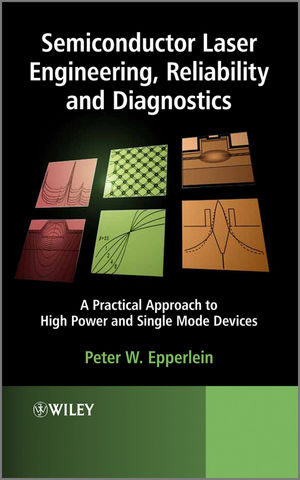
Semiconductor Laser Engineering, Reliability and Diagnostics
John Wiley & Sons Inc (Verlag)
978-1-119-99033-8 (ISBN)
Diode laser fundamentals are discussed, followed by an elaborate discussion of problem-oriented design guidelines and techniques, and by a systematic treatment of the origins of laser degradation and a thorough exploration of the engineering means to enhance the optical strength of the laser. Stability criteria of critical laser characteristics and key laser robustness factors are discussed along with clear design considerations in the context of reliability engineering approaches and models, and typical programs for reliability tests and laser product qualifications. Novel, advanced diagnostic methods are reviewed to discuss, for the first time in detail in book literature, performance- and reliability-impacting factors such as temperature, stress and material instabilities.
Further key features include:
practical design guidelines that consider also reliability related effects, key laser robustness factors, basic laser fabrication and packaging issues;
detailed discussion of diagnostic investigations of diode lasers, the fundamentals of the applied approaches and techniques, many of them pioneered by the author to be fit-for-purpose and novel in the application;
systematic insight into laser degradation modes such as catastrophic optical damage, and a wide range of technologies to increase the optical strength of diode lasers;
coverage of basic concepts and techniques of laser reliability engineering with details on a standard commercial high power laser reliability test program.
Semiconductor Laser Engineering, Reliability and Diagnostics reflects the extensive expertise of the author in the diode laser field both as a top scientific researcher as well as a key developer of high-power highly reliable devices. With invaluable practical advice, this new reference book is suited to practising researchers in diode laser technologies, and to postgraduate engineering students.
Dr. Peter W. Epperlein is Technology Consultant with his own semiconductor technology consulting business Pwe-PhotonicsElectronics-IssueResolution in the UK. He looks back at a thirty years career in cutting edge photonics and electronics industries with focus on emerging technologies, both in global and start-up companies, including IBM, Hewlett-Packard, Agilent Technologies, Philips/NXP, Essient Photonics and IBM/JDSU Laser Enterprise. He holds Pre-Dipl. (B.Sc.), Dipl. Phys. (M.Sc.) and Dr. rer. nat. (Ph.D.) degrees in physics, magna cum laude, from the University of Stuttgart, Germany. Dr. Epperlein is an internationally recognized expert in compound semiconductor and diode laser technologies. He has accomplished R&D in many device areas such as semiconductor lasers, LEDs, optical modulators, quantum well devices, resonant tunneling devices, FETs, and superconducting tunnel junctions and integrated circuits. His pioneering work on sophisticated diagnostic research has led to many world's first reports and has been adopted by other researchers in academia and industry. He authored more than seventy peer-reviewed journal papers, published more than ten invention disclosures in the IBM Technical Disclosure Bulletin, has served as reviewer of numerous proposals for publication in technical journals, and has won five IBM Research Division Awards. His key achievements include the design and fabrication of high-power, highly reliable, single mode diode lasers.
Preface xix
About the author xxiii
Part 1 Diode Laser Engineering 1
Overview 1
1 Basic diode laser engineering principles 3
Introduction 4
1.1 Brief recapitulation 4
1.1.1 Key features of a diode laser 4
1.1.1.1 Carrier population inversion 4
1.1.1.2 Net gain mechanism 6
1.1.1.3 Optical resonator 9
1.1.1.4 Transverse vertical confinement 11
1.1.1.5 Transverse lateral confinement 12
1.1.2 Homojunction diode laser 13
1.1.3 Double-heterostructure diode laser 15
1.1.4 Quantum well diode laser 17
1.1.4.1 Advantages of quantum well heterostructures for diode lasers 22
Wavelength adjustment and tunability 22
Strained quantum well lasers 23
Optical power supply 25
Temperature characteristics 26
1.1.5 Common compounds for semiconductor lasers 26
1.2 Optical output power – diverse aspects 31
1.2.1 Approaches to high-power diode lasers 31
1.2.1.1 Edge-emitters 31
1.2.1.2 Surface-emitters 33
1.2.2 High optical power considerations 35
1.2.2.1 Laser brightness 36
1.2.2.2 Laser beam quality factor M2 36
1.2.3 Power limitations 37
1.2.3.1 Kinks 37
1.2.3.2 Rollover 38
1.2.3.3 Catastrophic optical damage 38
1.2.3.4 Aging 39
1.2.4 High power versus reliability tradeoffs 39
1.2.5 Typical and record-high cw optical output powers 40
1.2.5.1 Narrow-stripe, single spatial mode lasers 40
1.2.5.2 Standard 100 μm wide aperture single emitters 42
1.2.5.3 Tapered amplifier lasers 43
1.2.5.4 Standard 1 cm diode laser bar arrays 44
1.3 Selected relevant basic diode laser characteristics 45
1.3.1 Threshold gain 45
1.3.2 Material gain spectra 46
1.3.2.1 Bulk double-heterostructure laser 46
1.3.2.2 Quantum well laser 47
1.3.3 Optical confinement 49
1.3.4 Threshold current 52
1.3.4.1 Double-heterostructure laser 52
1.3.4.2 Quantum well laser 54
1.3.4.3 Cavity length dependence 54
1.3.4.4 Active layer thickness dependence 56
1.3.5 Transverse vertical and transverse lateral modes 58
1.3.5.1 Vertical confinement structures – summary 58
Double-heterostructure 58
Single quantum well 58
Strained quantum well 59
Separate confinement heterostructure SCH and graded-index SCH (GRIN-SCH) 59
Multiple quantum well (MQW) 59
1.3.5.2 Lateral confinement structures 60
Gain-guiding concept and key features 60
Weakly index-guiding concept and key features 62
Strongly index-guiding concept and key features 63
1.3.5.3 Near-field and far-field pattern 64
1.3.6 Fabry–P´erot longitudinal modes 67
1.3.7 Operating characteristics 69
1.3.7.1 Optical output power and efficiency 72
1.3.7.2 Internal efficiency and optical loss measurements 74
1.3.7.3 Temperature dependence of laser characteristics 74
1.3.8 Mirror reflectivity modifications 77
1.4 Laser fabrication technology 81
1.4.1 Laser wafer growth 82
1.4.1.1 Substrate specifications and preparation 82
1.4.1.2 Substrate loading 82
1.4.1.3 Growth 83
1.4.2 Laser wafer processing 84
1.4.2.1 Ridge waveguide etching and embedding 84
1.4.2.2 The p-type electrode 84
1.4.2.3 Ridge waveguide protection 85
1.4.2.4 Wafer thinning and the n-type electrode 85
1.4.2.5 Wafer cleaving; facet passivation and coating; laser optical inspection; and electrical testing 86
1.4.3 Laser packaging 86
1.4.3.1 Package formats 87
1.4.3.2 Device bonding 87
1.4.3.3 Optical power coupling 89
1.4.3.4 Device operating temperature control 95
1.4.3.5 Hermetic sealing 95
References 96
2 Design considerations for high-power single spatial mode operation 101
Introduction 102
2.1 Basic high-power design approaches 103
2.1.1 Key aspects 103
2.1.2 Output power scaling 104
2.1.3 Transverse vertical waveguides 105
2.1.3.1 Substrate 105
2.1.3.2 Layer sequence 107
2.1.3.3 Materials; layer doping; graded-index layer doping 108
Materials 108
Layer doping 113
Layer doping – n-type doping 113
Layer doping – p-type doping 113
Graded-index layer doping 114
2.1.3.4 Active layer 114
Integrity – spacer layers 114
Integrity – prelayers 115
Integrity – deep levels 115
Quantum wells versus quantum dots 116
Number of quantum wells 119
2.1.3.5 Fast-axis beam divergence engineering 121
Thin waveguides 122
Broad waveguides and decoupled confinement heterostructures 122
Low refractive index mode puller layers 124
Optical traps and asymmetric waveguide structures 126
Spread index or passive waveguides 127
Leaky waveguides 128
Spot-size converters 128
Photonic bandgap crystal 130
2.1.3.6 Stability of the fundamental transverse vertical mode 133
2.1.4 Narrow-stripe weakly index-guided transverse lateral waveguides 134
2.1.4.1 Ridge waveguide 134
2.1.4.2 Quantum well intermixing 135
2.1.4.3 Weakly index-guided buried stripe 137
2.1.4.4 Slab-coupled waveguide 138
2.1.4.5 Anti-resonant reflecting optical waveguide 140
2.1.4.6 Stability of the fundamental transverse lateral mode 141
2.1.5 Thermal management 144
2.1.6 Catastrophic optical damage elimination 146
2.2 Single spatial mode and kink control 146
2.2.1 Key aspects 146
2.2.1.1 Single spatial mode conditions 147
2.2.1.2 Fundamental mode waveguide optimizations 150
Waveguide geometry; internal physical mechanisms 150
Figures of merit 152
Transverse vertical mode expansion; mirror reflectivity; laser length 153
2.2.1.3 Higher order lateral mode suppression by selective losses 154
Absorptive metal layers 154
Highly resistive regions 156
2.2.1.4 Higher order lateral mode filtering schemes 157
Curved waveguides 157
Tilted mirrors 158
2.2.1.5 Beam steering and cavity length dependence of kinks 158
Beam-steering kinks 158
Kink versus cavity length dependence 159
2.2.1.6 Suppression of the filamentation effect 160
2.3 High-power, single spatial mode, narrow ridge waveguide lasers 162
2.3.1 Introduction 162
2.3.2 Selected calculated parameter dependencies 163
2.3.2.1 Fundamental spatial mode stability regime 163
2.3.2.2 Slow-axis mode losses 163
2.3.2.3 Slow-axis near-field spot size 164
2.3.2.4 Slow-axis far-field angle 166
2.3.2.5 Transverse lateral index step 167
2.3.2.6 Fast-axis near-field spot size 167
2.3.2.7 Fast-axis far-field angle 168
2.3.2.8 Internal optical loss 170
2.3.3 Selected experimental parameter dependencies 171
2.3.3.1 Threshold current density versus cladding layer composition 171
2.3.3.2 Slope efficiency versus cladding layer composition 172
2.3.3.3 Slope efficiency versus threshold current density 172
2.3.3.4 Threshold current versus slow-axis far-field angle 172
2.3.3.5 Slope efficiency versus slow-axis far-field angle 174
2.3.3.6 Kink-free power versus residual thickness 174
2.4 Selected large-area laser concepts and techniques 176
2.4.1 Introduction 176
2.4.2 Broad-area (BA) lasers 178
2.4.2.1 Introduction 178
2.4.2.2 BA lasers with tailored gain profiles 179
2.4.2.3 BA lasers with Gaussian reflectivity facets 180
2.4.2.4 BA lasers with lateral grating-confined angled waveguides 182
2.4.3 Unstable resonator (UR) lasers 183
2.4.3.1 Introduction 183
2.4.3.2 Curved-mirror UR lasers 184
2.4.3.3 UR lasers with continuous lateral index variation 187
2.4.3.4 Quasi-continuous unstable regrown-lens-train resonator lasers 188
2.4.4 Tapered amplifier lasers 189
2.4.4.1 Introduction 189
2.4.4.2 Tapered lasers 189
2.4.4.3 Monolithic master oscillator power amplifiers 192
2.4.5 Linear laser array structures 194
2.4.5.1 Introduction 194
2.4.5.2 Phase-locked coherent linear laser arrays 194
2.4.5.3 High-power incoherent standard 1 cm laser bars 197
References 201
Part 2 Diode Laser Reliability 211
Overview 211
3 Basic diode laser degradation modes 213
Introduction 213
3.1 Degradation and stability criteria of critical diode laser characteristics 214
3.1.1 Optical power; threshold; efficiency; and transverse modes 214
3.1.1.1 Active region degradation 214
3.1.1.2 Mirror facet degradation 215
3.1.1.3 Lateral confinement degradation 215
3.1.1.4 Ohmic contact degradation 216
3.1.2 Lasing wavelength and longitudinal modes 220
3.2 Classification of degradation modes 222
3.2.1 Classification of degradation phenomena by location 222
3.2.1.1 External degradation 222
Mirror degradation 222
Contact degradation 223
Solder degradation 224
3.2.1.2 Internal degradation 224
Active region degradation and junction degradation 224
3.2.2 Basic degradation mechanisms 225
3.2.2.1 Rapid degradation 226
Features and causes of rapid degradation 226
Elimination of rapid degradation 229
3.2.2.2 Gradual degradation 229
Features and causes of gradual degradation 229
Elimination of gradual degradation 230
3.2.2.3 Sudden degradation 231
Features and causes of sudden degradation 231
Elimination of sudden degradation 233
3.3 Key laser robustness factors 234
References 241
4 Optical strength engineering 245
Introduction 245
4.1 Mirror facet properties – physical origins of failure 246
4.2 Mirror facet passivation and protection 249
4.2.1 Scope and effects 249
4.2.2 Facet passivation techniques 250
4.2.2.1 E2 process 250
4.2.2.2 Sulfide passivation 251
4.2.2.3 Reactive material process 252
4.2.2.4 N2IBE process 252
4.2.2.5 I-3 process 254
4.2.2.6 Pulsed UV laser-assisted techniques 255
4.2.2.7 Hydrogenation and silicon hydride barrier layer process 256
4.2.3 Facet protection techniques 258
4.3 Nonabsorbing mirror technologies 259
4.3.1 Concept 259
4.3.2 Window grown on facet 260
4.3.2.1 ZnSe window layer 260
4.3.2.2 AlGaInP window layer 260
4.3.2.3 AlGaAs window layer 261
4.3.2.4 EMOF process 261
4.3.2.5 Disordering ordered InGaP 262
4.3.3 Quantum well intermixing processes 262
4.3.3.1 Concept 262
4.3.3.2 Impurity-induced disordering 263
Ion implantation and annealing 263
Selective diffusion techniques 265
Ion beam intermixing 266
4.3.3.3 Impurity-free vacancy disordering 267
4.3.3.4 Laser-induced disordering 268
4.3.4 Bent waveguide 269
4.4 Further optical strength enhancement approaches 270
4.4.1 Current blocking mirrors and material optimization 270
4.4.1.1 Current blocking mirrors 270
4.4.1.2 Material optimization 272
4.4.2 Heat spreader layer; device mounting; and number of quantum wells 273
4.4.2.1 Heat spreader and device mounting 273
4.4.2.2 Number of quantum wells 273
4.4.3 Mode spot widening techniques 274
References 276
5 Basic reliability engineering concepts 281
Introduction 282
5.1 Descriptive reliability statistics 283
5.1.1 Probability density function 283
5.1.2 Cumulative distribution function 283
5.1.3 Reliability function 284
5.1.4 Instantaneous failure rate or hazard rate 285
5.1.5 Cumulative hazard function 285
5.1.6 Average failure rate 286
5.1.7 Failure rate units 286
5.1.8 Bathtub failure rate curve 287
5.2 Failure distribution functions – statistical models for nonrepairable populations 288
5.2.1 Introduction 288
5.2.2 Lognormal distribution 289
5.2.2.1 Introduction 289
5.2.2.2 Properties 289
5.2.2.3 Areas of application 291
5.2.3 Weibull distribution 291
5.2.3.1 Introduction 291
5.2.3.2 Properties 292
5.2.3.3 Areas of application 294
5.2.4 Exponential distribution 294
5.2.4.1 Introduction 294
5.2.4.2 Properties 295
5.2.4.3 Areas of application 297
5.3 Reliability data plotting 298
5.3.1 Life-test data plotting 298
5.3.1.1 Lognormal distribution 298
5.3.1.2 Weibull distribution 300
5.3.1.3 Exponential distribution 303
5.4 Further reliability concepts 306
5.4.1 Data types 306
5.4.1.1 Time-censored or time-terminated tests 306
5.4.1.2 Failure-censored or failure-terminated tests 307
5.4.1.3 Readout time data tests 307
5.4.2 Confidence limits 307
5.4.3 Mean time to failure calculations 309
5.4.4 Reliability estimations 310
5.5 Accelerated reliability testing – physics–statistics models 310
5.5.1 Acceleration relationships 310
5.5.1.1 Exponential; Weibull; and lognormal distribution acceleration 311
5.5.2 Remarks on acceleration models 312
5.5.2.1 Arrhenius model 313
5.5.2.2 Inverse power law 315
5.5.2.3 Eyring model 316
5.5.2.4 Other acceleration models 318
5.5.2.5 Selection of accelerated test conditions 319
5.6 System reliability calculations 320
5.6.1 Introduction 320
5.6.2 Independent elements connected in series 321
5.6.3 Parallel system of independent components 322
References 323
6 Diode laser reliability engineering program 325
Introduction 325
6.1 Reliability test plan 326
6.1.1 Main purpose; motivation; and goals 326
6.1.2 Up-front requirements and activities 327
6.1.2.1 Functional and reliability specifications 327
6.1.2.2 Definition of product failures 328
6.1.2.3 Failure modes, effects, and criticality analysis 328
6.1.3 Relevant parameters for long-term stability and reliability 330
6.1.4 Test preparations and operation 330
6.1.4.1 Samples; fixtures; and test equipment 330
6.1.4.2 Sample sizes and test durations 331
6.1.5 Overview of reliability program building blocks 332
6.1.5.1 Reliability tests and conditions 334
6.1.5.2 Data collection and master database 334
6.1.5.3 Data analysis and reporting 335
6.1.6 Development tests 336
6.1.6.1 Design verification tests 336
Reliability demonstration tests 336
Step stress testing 337
6.1.6.2 Accelerated life tests 339
Laser chip 339
Laser module 341
6.1.6.3 Environmental stress testing – laser chip 342
Temperature endurance 342
Mechanical integrity 343
Special tests 344
6.1.6.4 Environmental stress testing – subcomponents and module 344
Temperature endurance 345
Mechanical integrity 346
Special tests 346
6.1.7 Manufacturing tests 348
6.1.7.1 Functionality tests and burn-in 348
6.1.7.2 Final reliability verification tests 349
6.2 Reliability growth program 349
6.3 Reliability benefits and costs 350
6.3.1 Types of benefit 350
6.3.1.1 Optimum reliability-level determination 350
6.3.1.2 Optimum product burn-in time 350
6.3.1.3 Effective supplier evaluation 350
6.3.1.4 Well-founded quality control 350
6.3.1.5 Optimum warranty costs and period 351
6.3.1.6 Improved life-cycle cost-effectiveness 351
6.3.1.7 Promotion of positive image and reputation 351
6.3.1.8 Increase in customer satisfaction 351
6.3.1.9 Promotion of sales and future business 351
6.3.2 Reliability–cost tradeoffs 351
References 353
Part 3 Diode Laser Diagnostics 355
Overview 355
7 Novel diagnostic laser data for active layer material integrity; impurity trapping effects; and mirror temperatures 361
Introduction 362
7.1 Optical integrity of laser wafer substrates 362
7.1.1 Motivation 362
7.1.2 Experimental details 363
7.1.3 Discussion of wafer photoluminescence (PL) maps 364
7.2 Integrity of laser active layers 366
7.2.1 Motivation 366
7.2.2 Experimental details 367
7.2.2.1 Radiative transitions 367
7.2.2.2 The samples 369
7.2.2.3 Low-temperature PL spectroscopy setup 369
7.2.3 Discussion of quantum well PL spectra 371
7.2.3.1 Exciton and impurity-related recombinations 371
7.2.3.2 Dependence on thickness of well and barrier layer 373
7.2.3.3 Prelayers for improving active layer integrity 375
7.3 Deep-level defects at interfaces of active regions 376
7.3.1 Motivation 376
7.3.2 Experimental details 377
7.3.3 Discussion of deep-level transient spectroscopy results 382
7.4 Micro-Raman spectroscopy for diode laser diagnostics 386
7.4.1 Motivation 386
7.4.2 Basics of Raman inelastic light scattering 388
7.4.3 Experimental details 391
7.4.4 Raman on standard diode laser facets 394
7.4.5 Raman for facet temperature measurements 395
7.4.5.1 Typical examples of Stokes- and anti-Stokes Raman spectra 396
7.4.5.2 First laser mirror temperatures by Raman 398
7.4.6 Various dependencies of diode laser mirror temperatures 401
7.4.6.1 Laser material 402
7.4.6.2 Mirror surface treatment 403
7.4.6.3 Cladding layers; mounting of laser die; heat spreader; and number of active quantum wells 404
References 406
8 Novel diagnostic laser data for mirror facet disorder effects; mechanical stress effects; and facet coating instability 409
Introduction 410
8.1 Diode laser mirror facet studies by Raman 410
8.1.1 Motivation 410
8.1.2 Raman microprobe spectra 410
8.1.3 Possible origins of the 193 cm−1 mode in (Al)GaAs 412
8.1.4 Facet disorder – facet temperature – catastrophic optical mirror damage robustness correlations 413
8.2 Local mechanical stress in ridge waveguide diode lasers 416
8.2.1 Motivation 416
8.2.2 Measurements – Raman shifts and stress profiles 417
8.2.3 Detection of “weak spots” 419
8.2.3.1 Electron irradiation and electron beam induced current (EBIC) images of diode lasers 419
8.2.3.2 EBIC – basic concept 421
8.2.4 Stress model experiments 422
8.2.4.1 Laser bar bending technique and results 422
8.3 Diode laser mirror facet coating structural instability 424
8.3.1 Motivation 424
8.3.2 Experimental details 424
8.3.3 Silicon recrystallization by internal power exposure 425
8.3.3.1 Dependence on silicon deposition technique 425
8.3.3.2 Temperature rises in ion beam- and plasma enhanced chemical vapor-deposited amorphous silicon coatings 427
8.3.4 Silicon recrystallization by external power exposure –control experiments 428
8.3.4.1 Effect on optical mode and P/I characteristics 429
References 430
9 Novel diagnostic data for diverse laser temperature effects; dynamic laser degradation effects; and mirror temperature maps 433
Introduction 434
9.1 Thermoreflectance microscopy for diode laser diagnostics 435
9.1.1 Motivation 435
9.1.2 Concept and signal interpretation 437
9.1.3 Reflectance–temperature change relationship 439
9.1.4 Experimental details 439
9.1.5 Potential perturbation effects on reflectance 441
9.2 Thermoreflectance versus optical spectroscopies 442
9.2.1 General 442
9.2.2 Comparison 442
9.3 Lowest detectable temperature rise 444
9.4 Diode laser mirror temperatures by micro-thermoreflectance 445
9.4.1 Motivation 445
9.4.2 Dependence on number of active quantum wells 445
9.4.3 Dependence on heat spreader 446
9.4.4 Dependence on mirror treatment and coating 447
9.4.5 Bent-waveguide nonabsorbing mirror 448
9.5 Diode laser mirror studies by micro-thermoreflectance 451
9.5.1 Motivation 451
9.5.2 Real-time temperature-monitored laser degradation 451
9.5.2.1 Critical temperature to catastrophic optical mirror damage 451
9.5.2.2 Development of facet temperature with operation time 453
9.5.2.3 Temperature associated with dark-spot defects in mirror facets 454
9.5.3 Local optical probe 455
9.5.3.1 Threshold and heating distribution within near-field spot 455
9.6 Diode laser cavity temperatures by micro-electroluminescence 456
9.6.1 Motivation 456
9.6.2 Experimental details – sample and setup 456
9.6.3 Temperature profiles along laser cavity 457
9.7 Diode laser facet temperature – two-dimensional mapping 460
9.7.1 Motivation 460
9.7.2 Experimental concept 460
9.7.3 First temperature maps ever 460
9.7.4 Independent temperature line scans perpendicular to the active layer 461
9.7.5 Temperature modeling 462
9.7.5.1 Modeling procedure 463
9.7.5.2 Modeling results and discussion 465
References 466
Index 469
| Erscheint lt. Verlag | 7.3.2013 |
|---|---|
| Verlagsort | New York |
| Sprache | englisch |
| Maße | 160 x 236 mm |
| Gewicht | 771 g |
| Themenwelt | Naturwissenschaften ► Physik / Astronomie ► Optik |
| Technik ► Elektrotechnik / Energietechnik | |
| ISBN-10 | 1-119-99033-5 / 1119990335 |
| ISBN-13 | 978-1-119-99033-8 / 9781119990338 |
| Zustand | Neuware |
| Haben Sie eine Frage zum Produkt? |
aus dem Bereich


