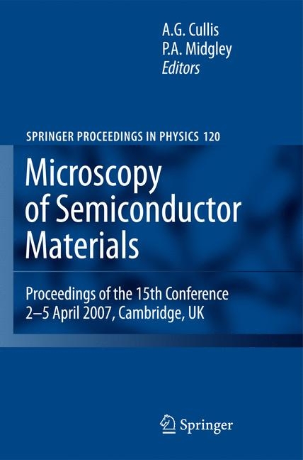
Microscopy of Semiconducting Materials 2007 (eBook)
XIV, 498 Seiten
Springer Netherland (Verlag)
978-1-4020-8615-1 (ISBN)
This volume contains invited and contributed papers presented at the conference on 'Microscopy of Semiconducting Materials' held at the University of Cambridge on 2-5 April 2007. The event was organised under the auspices of the Electron Microscopy and Analysis Group of the Institute of Physics, the Royal Microscopical Society and the Materials Research Society. This international conference was the fifteenth in the series that focuses on the most recent world-wide advances in semiconductor studies carried out by all forms of microscopy and it attracted delegates from more than 20 countries. With the relentless evolution of advanced electronic devices into ever smaller nanoscale structures, the problem relating to the means by which device features can be visualised on this scale becomes more acute. This applies not only to the imaging of the general form of layers that may be present but also to the determination of composition and doping variations that are employed. In view of this scenario, the vital importance of transmission and scanning electron microscopy, together with X-ray and scanning probe approaches can immediately be seen. The conference featured developments in high resolution microscopy and nanoanalysis, including the exploitation of recently introduced aberration-corrected electron microscopes. All associated imaging and analytical techniques were demonstrated in studies including those of self-organised and quantum domain structures. Many analytical techniques based upon scanning probe microscopies were also much in evidence, together with more general applications of X-ray diffraction methods.
Envisaged contents: The main topic areas are as follows: The characterisation of as-grown semiconductors in both bulk and thin film forms. The study of nanostructures of all types from quantum dots, wires, etc to nanotubes. The investigation of lattice defect and impurity behaviour in semiconducting materials. The study of the effects of semiconductor processing treatments
- oxidation, nitridation, ion implantation, annealing, silicidation, etc. The assessment of finished electronic devices, including studies of the influence of structural defects upon their behaviour and important new design features such as high/low k dielectrics, etc. The state of the art in analytical technique development from advances in FEGTEM nanoanalysis to exploitation of FIB milling for specimen preparation. Special conference sessions focused attention on recent advances in a number of areas of particular current interest, for example: Developments in the use of high resolution imaging and analytical transmission electron microscopy
- studies of bulk material, layers and interfaces. Advances in FIB milling and nanofabrication. The nature of epitaxial layers, superlattices and quantum well, wire and dot structures
- strain relaxation, defect introduction, morphological distortion, self-organisation, luminescence. Wide bandgap semiconductors, especially III-nitrides. The structures of dislocations and defect boundaries in semiconductors. Advances in SiGe/Si for device structures such as HBTs, MOSFETs, terahertz emitters, etc. Metal-semiconductor contacts and silicides. The effects of processing treatments using both conventional and transient techniques. The exploitation of advanced scanning techniques
-SEM-EBIC, SEM-CL, etc
-STM, AFM, SCM, BEEM, etc
| Erscheint lt. Verlag | 2.12.2008 |
|---|---|
| Reihe/Serie | Springer Proceedings in Physics | Springer Proceedings in Physics |
| Zusatzinfo | XIV, 498 p. |
| Verlagsort | Dordrecht |
| Sprache | englisch |
| Themenwelt | Naturwissenschaften ► Physik / Astronomie ► Elektrodynamik |
| Technik ► Elektrotechnik / Energietechnik | |
| Technik ► Maschinenbau | |
| Schlagworte | Canopus • crystals and superlattices • electron microscopy • Integrated circuit • microcharacterization techniques • nanoscience and nanostructures • quantum dot • semiconductor • semiconductor materials • semiconductor processing treatments • Thin film • Transmission Electron Microscopy |
| ISBN-10 | 1-4020-8615-6 / 1402086156 |
| ISBN-13 | 978-1-4020-8615-1 / 9781402086151 |
| Haben Sie eine Frage zum Produkt? |
Größe: 104,8 MB
DRM: Digitales Wasserzeichen
Dieses eBook enthält ein digitales Wasserzeichen und ist damit für Sie personalisiert. Bei einer missbräuchlichen Weitergabe des eBooks an Dritte ist eine Rückverfolgung an die Quelle möglich.
Dateiformat: PDF (Portable Document Format)
Mit einem festen Seitenlayout eignet sich die PDF besonders für Fachbücher mit Spalten, Tabellen und Abbildungen. Eine PDF kann auf fast allen Geräten angezeigt werden, ist aber für kleine Displays (Smartphone, eReader) nur eingeschränkt geeignet.
Systemvoraussetzungen:
PC/Mac: Mit einem PC oder Mac können Sie dieses eBook lesen. Sie benötigen dafür einen PDF-Viewer - z.B. den Adobe Reader oder Adobe Digital Editions.
eReader: Dieses eBook kann mit (fast) allen eBook-Readern gelesen werden. Mit dem amazon-Kindle ist es aber nicht kompatibel.
Smartphone/Tablet: Egal ob Apple oder Android, dieses eBook können Sie lesen. Sie benötigen dafür einen PDF-Viewer - z.B. die kostenlose Adobe Digital Editions-App.
Buying eBooks from abroad
For tax law reasons we can sell eBooks just within Germany and Switzerland. Regrettably we cannot fulfill eBook-orders from other countries.
aus dem Bereich


