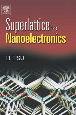
Superlattice to Nanoelectronics
Elsevier Science Ltd (Verlag)
978-0-08-044377-5 (ISBN)
- Titel erscheint in neuer Auflage
- Artikel merken
Superlattice to Nanoelectronics provides a historical overview of the early work performed by Tsu and Esaki, to orient those who want to enter into this nanoscience. It describes the fundamental concepts and goes on to answer many questions about todays 'Nanoelectronics'. It covers the applications and types of devices which have been produced, many of which are still in use today. This historical perspective is important as a guide to what and how technology and new fundamental ideas are introduced and developed. The author communicates a basic understanding of the physics involved from first principles, whilst adding new depth, using simple mathematics and explanation of the background essentials. Topics covered include* Introductory materials * Superlattice, Bloch oscillations and transport * Tunneling in QWs to QDs * Optical properties: optical transitions, size dependent dielectric constant, capacitance and doping * Quantum devices: New approaches without doping and heterojunctions - quantum confinement via geometry and multipole electrodes. Issues of robustness, redundancy and I/O.Researchers, course students and research establishments should read this book, written by the leading expert in nanoelectronics and superlattices.
Dr. R. Tsu started his professional career at the Bell Telephone Laboratories, Murray Hill, NJ, 1961, working on the theory and experiments related to electron-phonon interaction in piezoelectric solids. He became a close collaborator of Leo Esaki (Nobel Laureate in 1973) at IBM T.J. Watson Research Center where he joined in 1966, working on theory and experiments of optical- and transport-properties, band structures, in solids, and material characterization. A man-made semiconductor superlattice and modulation doping were conceived jointly with Esaki, in 1969, which led to a rapid development of man-made quantum materials and quantum structures eventually evolved into the present day quantum dots. His original formulation of tunneling through multiple man-made heterojunctions is widely accepted in nearly all aspects of resonant tunneling devices reaching Tera-Hertz, thus far being the fastest device to date. The theory and experiments of man-made superlattices and resonant tunneling through a quantum well led to his outstanding contribution award from IBM Research in 1975 and later in 1985, to sharing the International New Materials Prize of the American Physical Society with Esaki and Chang. In 1979, he became the head of Materials Research at Energy Conversion Devices, Inc., in charge of the study on the formation and structure of amorphous silicon. His major contributions involve the determination of bond angle distribution from Raman scattering and optical absorption measurements and experimental determination of conductivity percolation. In 1985, he became the head of the amorphous silicon research group at the Solar Energy Research Institute (now NREL) as a principal scientist, working on amorphous Si/Ge and Si/C alloys, showing that the famous Tauc's plot may be theoretically derived without adjustable parameters. In 1975, as the recipient of the Alexander von Humboldt award, he took a year sabbatical at Max Planck Institute for Solid State Physics in
Preface
Introduction
CHAPTER 1
SUPERLATTICE
1.1 The Birth of the Man-Made Superlattice
1.2 A Model for the Creation of Man-Made Energy Bands
1.3 Transport Properties of a Superlattice 6
1.4 More Rigorous Derivation of the Negative
Differential Conductance
1.5 Response of a Time-Dependent Electric Field
1.6 NDC from the Hopping Model and Electric Field
Induced Localization
1.7 Experiments
1.8 Type II Superlattice
1.9 Physical Realization and Characterization of a Superlattice
1.10 Summary
References
CHAPTER 2
RESONANT TUNNELING VIA MAN-MADE QUANTUM WELL STATES
2.1 The Birth of Resonant Tunneling
2.2 Some Fundamentals
2.3 Conductance from the Tsu–Esaki Formula
2.4 Tunneling Time from the Time-Dependent Schro¨dinger Equation
2.5 Damping in Resonant Tunneling
2.6 Very Short ‘ and w for an Amorphous Quantum Well
2.7 Self-Consistent Potential Correction of DBRT
2.8 Experimental Confirmation of Resonant Tunneling
2.9 Instability in RTD
2.10 Summary
References
CHAPTER 3
OPTICAL PROPERTIES AND RAMAN SCATTERING IN MAN-MADE QUANTUM SYSTEMS
3.1 Optical Absorption in a Superlattice
3.2 Photoconductivity in a Superlattice
3.3 Raman Scattering in a Superlattice and Quantum Well
3.4 Summary
References
CHAPTER 4
DIELECTRIC FUNCTION AND DOPING OF A SUPERLATTICE
4.1 Dielectric Function of a Superlattice and a Quantum Well
4.2 Doping a Superlattice
4.3 Summary
References
CHAPTER 5
QUANTUM STEP AND ACTIVATION ENERGY
5.1 Optical Properties of Quantum Steps
5.2 Determination of Activation Energy in Quantum Wells
5.3 Summary
References
CHAPTER 6
SEMICONDUCTOR ATOMIC SUPERLATTICE (SAS)
6.1 Silicon-Based Quantum Wells
6.2 Si-Interface Adsorbed Gas (IAG) Superlattice
6.3 Amorphous Silicon/Silicon Oxide Superlattice
6.4 Silicon–Oxygen (Si–O) Superlattice
6.5 Estimate of the Band-Edge Alignment Using Atomic States
6.6 Estimate of the Band-Edge Alignment with HOMO–LUMO
6.7 Estimation of Strain from a Ball and Stick Model
6.8 Electroluminescence and Photoluminescence
6.9 Transport through a Si–O Superlattice
6.10 Comparison of a Si–O Superlattice and a Ge–Si Monolayer Superlattice
6.11 Summary
References
CHAPTER 7
Si QUANTUM DOTS
7.1 Energy States of Silicon Quantum Dots
7.2 Resonant Tunneling in Silicon Quantum Dots
7.3 Slow Oscillations and Hysteresis
7.4 Avalanche Multiplication from Resonant Tunneling
7.5 Influence of Light and Repeatability under Multiple Scans
7.6 Summary
References
CHAPTER 8
CAPACITANCE, DIELECTRIC CONSTANT AND DOPING
QUANTUM DOTS
8.1 Capacitance of Silicon Quantum Dots
8.2 Dielectric Constant of a Silicon Quantum Dot
8.3 Doping a Silicon Quantum Dot
8.4 Summary
References
CHAPTER 9
POROUS SILICON
9.1 Porous Silicon—Light Emitting Silicon
9.2 Porous Silicon—Other Applications
9.3 Summary
References
CHAPTER 10
SOME NOVEL DEVICES
10.1 Cold Cathode
10.2 Saturation Intensity of PbS Quantum Dots
10.3 Multipole Electrode Heterojunction Hybrid Structures
10.4 Some Fundamental Issues: Mainly Difficulties
10.5 Comments on Quantum Computing
10.6 Summary
References
CHAPTER 11
QUANTUM IMPEDANCE OF ELECTRONS
11.1 Landauer Conductance Formula
11.2 Electron Quantum Waveguide (EQW)
11.3 Wave Impedance of Electrons
11.4 Summary
References
CHAPTER 12
NANOELECTRONICS: WHERE ARE YOU?
References
| Erscheint lt. Verlag | 4.4.2005 |
|---|---|
| Verlagsort | Oxford |
| Sprache | englisch |
| Maße | 156 x 234 mm |
| Gewicht | 770 g |
| Themenwelt | Technik ► Elektrotechnik / Energietechnik |
| ISBN-10 | 0-08-044377-X / 008044377X |
| ISBN-13 | 978-0-08-044377-5 / 9780080443775 |
| Zustand | Neuware |
| Haben Sie eine Frage zum Produkt? |
aus dem Bereich
