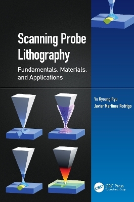
Scanning Probe Lithography
Taylor & Francis Ltd (Verlag)
978-1-032-12215-1 (ISBN)
Introduces historical background of SPL, including evolution of the technique and tools
Explains the mechanism of sample modification/manipulation, types of AFM tips, technical parts of the experimental setup, and materials on which the technique can be applied
Shows the different types of devices and structures fabricated by SPL, together with the processing steps
Contains a complete and state-of-the art package of examples and different approaches, performed by different international research groups
Summarizes strengths, limitations, and potential of SPL
Dr. Yu Kyoung Ryu is a postdoctoral researcher at Instituto de Sistemas Optoelectrónicos y Microtecnología (Universidad Politécnica de Madrid). She received a Physics degree from Universidad Complutense de Madrid and PhD from Instituto de Ciencia de Materiales de Madrid (ICMM, CSIC), under the supervision of Prof. Ricardo Garcia. She did a postdoctoral stay at IBM Research Zurich in the group of Dr. Armin Knoll (2016–2017) and a postdoctoral stay at ICMM (CSIC) in the group of Dr. Andrés Castellanos-Gomez (2019–2020). She has published 21 peer-reviewed articles in international journals (including ACS Nano, Nano Letters, Physical Review Letters, 2D Materials) and 3 book chapters. Prof. Javier Martinez Rodrigo is Vice Principal of the Instituto de Sistemas Optoelectrónicos y Microtecnología (ISOM) at Universidad Politécnica de Madrid (UPM) and coordinator of the ICTS Clean Rooms network for Micro and Nanofabrication MICRONANOFABs (www.micronanofabs.org). He achieved the PhD degree in Physics in 2002 and also an Electronic Engineering degree from Universidad de Valladolid. He worked as postdoctoral researcher at the Lawrence Berkeley National Laboratory (USA) in 2003 and later he was appointed as CSIC researcher at the Madrid Institute of Microelectronics, where his main topic was the fabrication of devices and the development of high-throughput strategies based on oxidation scanning probe lithography. In 2011 he became I3 Professor at UPM. His research interest is focused in the development of nanoelectronic devices fabricated with graphene or other 2D materials for energy applications. He has published more than 30 peer-reviewed articles in international journals (including Nature Nanotechnology, Advanced Materials, Nano Letters) and 1 book chapter. He holds 2 patents.
1. Historical Background and Positioning in the Lithography Roadmap. 2. Basic Concepts and Modalities. 3. Mechanical Scanning Probe Lithography. 4. Dip Pen Nanolithography. 5. Field Emission Scanning Probe Lithography. 6. Oxidation Scanning Probe Lithography. 7. Thermal Scanning Probe Lithography. 8. Lithography Using an Scanning Tunneling Microscope. 9. High Throughput Strategies.
| Erscheint lt. Verlag | 30.6.2024 |
|---|---|
| Reihe/Serie | Emerging Materials and Technologies |
| Zusatzinfo | 17 Line drawings, black and white; 43 Halftones, black and white; 60 Illustrations, black and white |
| Verlagsort | London |
| Sprache | englisch |
| Maße | 156 x 234 mm |
| Themenwelt | Technik ► Elektrotechnik / Energietechnik |
| Technik ► Maschinenbau | |
| Technik ► Umwelttechnik / Biotechnologie | |
| ISBN-10 | 1-032-12215-3 / 1032122153 |
| ISBN-13 | 978-1-032-12215-1 / 9781032122151 |
| Zustand | Neuware |
| Haben Sie eine Frage zum Produkt? |
aus dem Bereich


