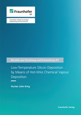
Low-Temperature Silicon Deposition by Means of Hot-Wire Chemical Vapour Deposition
Seiten
This work showcases the development of an industrially relevant process for the low substrate-temperature deposition of silicon for MEMS applications. This opens possibilities to deposit MEMS structures directly onto pre-fabricated ASICs, in addition to temperature sensitive substrates. Additionally, this work details the development of an advanced simulation model to optimize film crystallinity, without the need for increased temperatures.
In this work, a low substrate temperature silicon deposition process by means of hot-wire chemical vapor deposition was developed. This process was developed in order to facilitate silicon deposition directly onto a pre-fabricated application-specific integrated circuit (ASIC).
To further understand the parameter interactions and optimize the processes, an advanced model of the gas-phase and surface reactions in the HWCVD process was developed. By comparing the simulation model to experimental results, a clear correlation between the resulting film crystallinity and the simulated absorption rates of high surface mobility species (especially SiH3) has been observed and interpreted. These films were then deposited onto substrates with pre-fabricated NMOS structures, and then were subject to structuring and release processes.
The results of this work highlight the development of an advanced simulation model to provide new industrially relevant insights into HWCVD silicon. In addition, the low-substrate temperature process opens new possibilities for reductions in size of MEMS and ASIC integrated devices.
| Erscheinungsdatum | 24.06.2022 |
|---|---|
| Reihe/Serie | Berichte aus Forschung und Entwicklung IST ; 47 |
| Zusatzinfo | num., mostly col. illus. |
| Verlagsort | Stuttgart |
| Sprache | englisch |
| Maße | 148 x 210 mm |
| Themenwelt | Naturwissenschaften ► Physik / Astronomie ► Hochenergiephysik / Teilchenphysik |
| Technik ► Elektrotechnik / Energietechnik | |
| Technik ► Maschinenbau | |
| Schlagworte | B • HWCVD • Materials Scientists • MEMS • Physicists • Silicon • Simulation |
| ISBN-10 | 3-8396-1820-7 / 3839618207 |
| ISBN-13 | 978-3-8396-1820-2 / 9783839618202 |
| Zustand | Neuware |
| Haben Sie eine Frage zum Produkt? |
Mehr entdecken
aus dem Bereich
aus dem Bereich
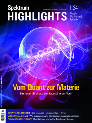
Neue Sicht auf die Bausteine der Welt
Buch (2024)
Spektrum der Wissenschaft (Verlag)
9,80 €


