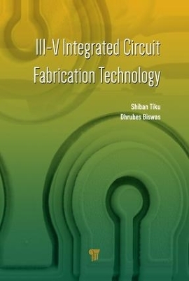
III-V Integrated Circuit Fabrication Technology
Pan Stanford Publishing Pte Ltd (Verlag)
978-981-4669-30-6 (ISBN)
Shiban Tiku is an electrical engineer from Kashmir University, India, an M. Tech. from IIT Kanpur, India, and a PhD in materials science from the University of Southern California, Los Angeles. Dr. Tiku started work in GaAs ICs at Texas Instruments, Dallas, and has been with the Rockwell Semiconductor Division, from which Skyworks, California, was spun off, for over 20 years, first in process development and then in process engineering and yield engineering, covering design, layout, wafer fabrication, and back-end processing. He has worked on epigrowth, ion implantation, thin-film deposition, FET- and HBT-type device processing, piezoelectric devices, etc., and is currently in charge of new process/product introduction at Skyworks. He has served on the CS MANTECH technical committee for over 10 years and is now on the executive committee as the university liaison. He has published numerous papers and is the (co)author of 15 patents. Dhrubes Biswas is an electrical engineer from IIT Kharagpur, India, and an MS and PhD in engineering (electronic devices and materials) from the University of Illinois, Urbana-Champaign. Prof. Biswas has made significant contributions to gas-source molecular beam epitaxy and played an instrumental role in establishing and advising strategic technology ventures in wireless communication and optical networking electronics worldwide. Currently at IIT Kharagpur, he is the professor of electronics and electrical communication engineering and a professor at Rajendra Mishra School of Engineering Entrepreneurship. He is deeply involved in the integration of III–V electronics/optical front-end devices epitaxially on silicon for high-performance systems. He has authored over 170 technical papers and books and holds numerous patents. He is a senior member of the Institute of Electrical Engineers (IEEE) and a member of Tau Beta Pi and Phi Kappa Phi.
Semiconductor fundamentals. GaAs devices. Phase diagrams and crystal growth. Epitaxy. Photolithography. Wet etching. Cleaning and passivation. Plasma processing and dry etching. Deposition. Ion implantation and device isolation. Diffusion. Ohmic contacts. Schottky diodes and FET processing. HEMT process. HBT processing. BiFET and BiHEMT processing. MOSFET processing. Passive components. Interconnect technology. Backside processing and wafer bumping. Electroplating. Measurements and characterization. Reliability. GaN devices and R F MEMs.
| Zusatzinfo | 364 Illustrations, color; 37 Illustrations, black and white |
|---|---|
| Verlagsort | Singapore |
| Sprache | englisch |
| Maße | 152 x 229 mm |
| Gewicht | 1480 g |
| Themenwelt | Naturwissenschaften ► Physik / Astronomie ► Optik |
| Technik ► Elektrotechnik / Energietechnik | |
| Technik ► Maschinenbau | |
| ISBN-10 | 981-4669-30-X / 981466930X |
| ISBN-13 | 978-981-4669-30-6 / 9789814669306 |
| Zustand | Neuware |
| Haben Sie eine Frage zum Produkt? |
aus dem Bereich


